 Written by
Lucas Teske
Written by
Lucas Teske
on
This is a WIP document with my research about these LYD6168 chinese panels.
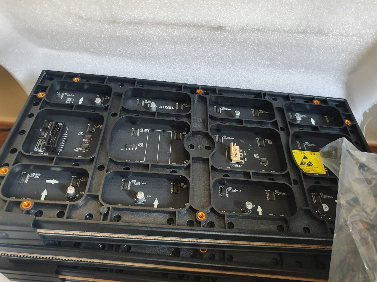
Everything started when I bought 6 of these panels (thanks to my supporters at twitch) for the Big Gate Boy project (a gigantic gameboy). I previously played with some other chinese panels with FM6126 and FM6127 chips, which although needed an FPGA to be able to display 18 bit color, worked nice.
Then I got the suprise that the 6 panels (which were not cheap for Brazillian standards) were a totally different chip: LYD6168
The thing that scared me about it was that besides knowing the LYD was a short for Leyard, there were actually zero information about the chip on the internet. I spend some of the live streams together with my supporters trying to find a datasheet or any info about the chip (searching even in chinese search engines). The only information we got was S-PWM. Also any code from the internet to control HUB75 panels, didn”t even lit the panel. I couldn’t be sure if my panels were dead or just were completely different than anything.
I tried to reach Leyard from china, Leyard from Brazil. But chinese leyard just ignored me, and Brazillian Leyard said they don’t know any LYD6168 panel. I also tried to reach the Chinese Seller and he said it is compatible with my Colorlight Hub 5A-75B board.
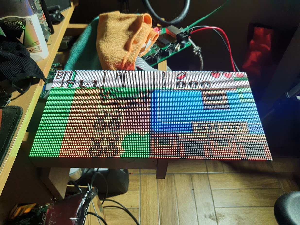
Funny enough, I even got the original chinese software to test it and after a while trying and failing (because the seller just said “it works”) I discovered that for S-PWM chips, there was another firmware for the FPGA.
The software for upgrading can be found at colorlight website: Colorlight LEDUpgrade V3.0. The firmware can be upgraded through network, but the cable should be connected directly to you ethernet card. I even tried using a USB 3.0 Gigabit card, and it didn’t work.
Also since the 5A-75B Ethernet clocks are fixed, it will only work on gigabit ethernet
After some trouble to get it working, I managed to upgrade it with a S-PWM Ready firmware which was at least trying to display something. Funny enough in Colorlight LED software, selecting the LYD6168 preset doesn’t work. I had to test manually every supported controller to see which one displayed the image correctly. The LYD6168 seens to display something but it was completely wrong. Finally I found out that LYD6168 panel correspond to MBI5153 made by Macroblocks and that Leyard does silicon OEM of their chips. Sadly, some people reported that their LYD6168 chips worked as a ICN2053 (which it doesn’t here). That probably means leyard just threw shit at the fan by selling the same IC package with different silicon inside.
Since my steps to find out which controller the panel had is probably usefull for future use, I will list my steps to get this panel working.
MBI5153
The good thing about MBI5153 that there is a datasheet available. Reading a bit the datasheet, we can see that they’re totally different than FM6126/6127 chips. The 6126 chips didn’t had any controller internally and were basically some fancy shift-registers. The MBI5153 are a complete different thing: The PWM are embedded, and the chip can fit the whole frame of scanlines inside it. Look at this:

So here we have a 14-bit counter for 16 bit comparators which outputs PWM for 16 outputs, which means we have 14-bit per color control. So after that data is latched into the MB5153, it will generate the led brightness by itself. That enables low speed microcontrollers to control that.
Also, they can hold up to 32 scanlines, which means my 128x64 panel can hold an entire frame. This means if I want to display a static image, I can just “send” the image to the panel, and keep pulsing the GCLK signal to display the image and controlling the line address bits for changing the scanlines. The chip also holds two frame-buffers which are switch using a V-SYNC command. That allows you to write the next frame while displaying the current one without aliasing the image.
The control commands are pretty similar to ICN2053, it is only controlled by two pins: LE and DCLK. Basically you clock the DCLK pins for 16 clocks with last N clocks with the LE asserted. The N tells you which command it will execute. Some commands need a pre-activation (which is another command). The commands are on the table below.
| # | Command Name | Need Pre-active | DCLK | Action |
| 1 | Data Latch / stop error detect | N | 1 | Latches the data to internal buffer |
| 2 | VSYNC | N | 2 | Switches the internal buffers |
| 3 | Write Configuration 1 | Y | 4 | Latches the data to register 1 |
| 4 | Read Configuration 1 | N | 5 | Reads the data from register 1 |
| 5 | Start compulsory error detect | N | 7 | Starts the compulsory LED open detect |
| 6 | Write Configuration 2 | Y | 8 | Latches the data to register 2 |
| 7 | Read Configuration 2 | N | 9 | Reads the data from register 2 |
| 8 | Software Reset | N | 10 | Resets the entire IC except config |
| 9 | Pre-Active | N | 14 | Enables write to registers |
Besides that, when clocking DCLK the chip is continuously reading the SDI pin and outputing data to SDO.
- For the commands 2,4,5,7,8,9 the SDI should be tied low.
- For commands 1,3,6 the
SDIis used for latching the data. - For commands 4,7 the
SDOwill output the data in next 16 clocks after finishing the command. The LE should be kept low. - The
LEis sampled at rising-edge ofDCLK - For any command that requires data to be sent to the chips, you should only issue
LEin the last 16 bit group- Since data is shifted across all devices, the data for the last chip in the chain is sent first.
- If you want to send the same data for all devices, you need to repeat the 16 bit group for every device
- Data is MSB First
For the diagrams below, I assume Samples starting at 1 (so 1 to 16 range).
DATA (N=1)
MBI5153 latches data to internal SRAM using 16 bits. But the PWM memory is “vertical” and the latch is “horizontal”. So when you latch data, you’re latching one bit from each channel. So the latch actually sends one bit per channel.
Assuming channels: A,B,C,D,E,F,G,H,I,J,K,L,M,N,O,P and bit 0 from channel A being A0.
VSync (N=2)
Switch internal screen buffer. The MBI5153 can hold two buffers of the entire image. So you can write one buffer and display another simultaneously.
Write Configuration Register 1 (N=4)
Should issue Pre-Active Command first.
Write Configuration Register 2 (N=8)
Should issue Pre-Active Command first.