on
Big Gate Boy
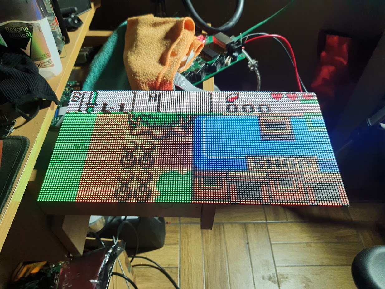
An open FPGA experiment that rebuilds the Game Boy in programmable logic and aims it at a gloriously oversized six-panel display.
Game Boy, rebuilt gate by gate.
Big Gate Boy explores a Game Boy-compatible CPU in Verilog for a Lattice ECP5, with six LED panels as the oversized display target. The source, tests, live sessions, and panel reverse engineering are collected here.
- CPU core and opcode map
- Assembly tests
- Panel reverse engineering
- Six-panel display target
Explore the build
Start with the layer that interests you: processor logic, unusual display hardware, recorded sessions, or source code.
CPU core and instruction map
Read the opcode conventions, register groups, ALU operations, and instruction map used while implementing the core.
Open the microcode referenceLYD6168 panel research
Follow the investigation that identified the undocumented LYD6168 panels as MBI5153-compatible hardware.
Read the panel investigationDevelopment sessions
Watch the project take shape in the recorded livestream sessions, from CPU work to hardware experiments.
Open the YouTube playlistVerilog, tests, and tooling
Browse the CPU modules, ALU and register-bank test benches, assembly test programs, constraints, and build tooling.
View the repositoryDisplay research notes
Practical references produced while turning six unfamiliar LED panels into usable project hardware.
- Identify and test the panel controller A step-by-step path through the vendor software and driver-IC detection process.
- Change the receiver-card FPGA firmware Notes for loading the S-PWM-capable firmware required by these panels.
- MBI5153 controller datasheet The controller reference that made the LYD6168 behavior understandable.