Reverse Engineering the AIR105 Bootrom - A Deep Dive into the MH1903S Boot Process
 Written by
Mister Maluco
Written by
Mister Maluco
on
Reverse Engineering the AIR105 Bootrom: A Deep Dive into the MH1903S Boot Process
The AIR105 is a secure microcontroller built around the MH1903S core — an ARM Cortex-M4F processor running at 168 MHz, designed for payment terminals and other security-critical embedded applications. It features hardware cryptography (SM2/SM3/SM4, AES, RSA-2048, SHA-256/384/512), OTP (One-Time Programmable) memory for key storage — though as we’ll see, the bootrom can write to OTP regions via the UART protocol, so it’s better thought of as controlled-access storage rather than truly write-once — on-the-fly flash encryption via a cache encryption engine, and a battery-backed key processing unit (BPU).
This article documents the complete boot process of its immutable bootrom, reverse engineered from the raw binary using Ghidra. We’ll trace the execution path from the reset vector all the way through to launching user firmware, covering the security lifecycle, the UART download protocol, firmware validation, and the differences between development and production devices.
The Bootrom
The bootrom is approximately 200 KB of Thumb-2 code mapped at address 0x00000000. It is factory-masked and cannot be modified. On reset, the Cortex-M processor reads the vector table from this address:
| Offset | Value | Purpose |
|---|---|---|
0x00 |
0x200D0120 |
Initial stack pointer |
0x04 |
0x00000329 |
Reset handler (Thumb bit set) |
0x08 |
0x0000021D |
NMI handler |
0x0C |
0x0000021D |
HardFault handler |
The reset vector points to 0x00000328, the entry point into the bootrom’s main logic.
Phase 1: Reset Vector and Early Startup
ResetHandler (0x00000328)
The reset handler is minimal:
void ResetHandler(void) {
    NVIC.SCB.VTOR = 0x0;     // Vector table offset = 0 (bootrom)
    _start();                 // Never returns
}
It sets the Vector Table Offset Register to point at the bootrom’s own vector table (address 0x0) and immediately calls _start.
_start (0x000000FC)
The _start function performs the standard C runtime initialization: it sets the stack pointer, zeroes the .bss section, copies initialized data from flash to RAM, and then calls _start2.
_start2 (0x0000277C)
This function walks a constructor table — an array of {function_ptr, arg0, arg1, arg2} entries located between 0x0001FA88 and the end of the table. Each entry’s function is called in order, performing static initializations before the main boot logic begins:
void _start2(void) {
    for (ptr = &ctorTable_start; ptr < &ctorTable_end; ptr++) {
        (*ptr->function)(ptr->arg0, ptr->arg1, ptr->arg2);
    }
    bootMain();    // Never returns
}
After all constructors run, control passes to bootMain — the heart of the bootrom.
Phase 2: bootMain — The Orchestrator
bootMain (0x00012944)
The real bootMain (not to be confused with the thin trampoline at 0x00000104) orchestrates the entire boot sequence:
void bootMain(void) {
    // 1. Enable FPU
    NVIC.SCB.CPACR |= 0xF00000;

    // 2. Phase marker and hardware init
    FUN_0001d404(0);
    InitializeHardware();
    ConfigureQSPIFlash(0);
    init_boot_marker();
    FUN_0001d404(1);

    // 3. Determine security state from OTP
    uVar2 = get_boot_state();

    // 4. Attempt UART/USB download (with timeout)
    HandshakeStateMachine(uVar2);

    // 5. Try booting from internal flash
    uVar3 = TryBoot(uVar2, &MH_FLASH_BASE);
    DAT_20020118 = uVar3 | 0x55550000;

    // 6. Try booting from external flash (XIP region)
    uVar2 = TryBoot(uVar2, &DAT_20020000);
    DAT_2002011c = uVar2 | 0x66660000;

    // 7. Nothing worked --- increment boot counter and restart
    SYSCTRL_BASE.RSVD_POR |= 0x55;
    Restart(bootCounter << 1, 0);   // Never returns
}
The boot strategy is straightforward:
- Initialize hardware — clocks, UART, QSPI flash, TRNG.
- Read security configuration from OTP memory.
- Listen for a download command over UART/USB for a limited time window.
- Try to boot from internal flash (built-in QSPI).
-
Try to boot from external flash (memory-mapped XIP region at
0x20020000). - Restart if neither flash source contains valid firmware.
The Restart() function is the bootrom’s universal error handler. It increments a boot-attempt counter in the SYSCTRL_BASE.RSVD_POR register, waits a configurable delay, then triggers a soft reset via SYSCTRL_BASE.SOFT_RST2 = 0x80000000. On production devices, it also disables JTAG (TST_BASE.TST_ROM = 0).
Phase 3: Hardware Initialization
InitializeHardware (0x00002C28)
void InitializeHardware(void) {
    ConfigureCaches();                              // Enable I/D caches
    SYSCTRL_PLLConfig(SYSCTRL_PLL_168MHz);          // Set PLL to 168 MHz
    SYSCTRL_PLLDivConfig(1);                        // PLL divider
    SYSCTRL_HCLKConfig(0);                          // AHB divider = 1 (168 MHz)
    SYSCTRL_PCLKConfig(1);                          // APB divider = 2 (84 MHz)
    SYSCTRL_APBPeriphClockCmd(0xa4300001, ENABLE);  // Enable APB peripherals
    SYSCTRL_APBPeriphResetCmd(0xa4300001, 1);       // Reset them
    SYSCTRL_APBPeriphClockCmd(0x30000001, ENABLE);  // Enable AHB peripherals
    SYSCTRL_AHBPeriphResetCmd(0x30000001, ENABLE);  // Reset them
    SYSCTRL_AHBPeriphResetCmd(0x10000000, DISABLE); // Release crypto from reset
    ConfigurePortC();                               // GPIO port C setup
    EnableUART3();                                  // Secondary UART
    TRNG_Start(TRNG0);                              // Start True Random Number Generator
    EnableUSBIRQ();                                 // USB interrupts
    ConfigureUART0(115200, 0);                      // Primary UART at 115200 baud
    ConfigureInterrupts();                          // NVIC setup
}
The system comes up at 168 MHz with all cryptographic hardware enabled and the TRNG already seeded. UART0 is configured at 115200 baud — this is the primary interface for firmware download.
Phase 4: Security State Determination
Before doing anything security-sensitive, the bootrom must determine what kind of device it’s running on. This is controlled by OTP memory values. Despite the “One-Time Programmable” name, the bootrom provides commands to write to OTP through the UART download protocol (via WriteFlashOption, ImportSmKey, WritePatch, etc.), with an unlock mechanism (InitializeOTPUnlockKeys) that gates access. So OTP here is more accurately “controlled-access storage” — writable under specific conditions, but not freely modifiable by arbitrary code.
get_boot_state (0x00005048)
uint get_boot_state(void) {
    __aeabi_memclr(&encryptKey, 32);        // Clear encryption key
    apply_otp_register_patches(0);           // Apply OTP register overrides
    ConfigureInterrupts();

    version = determine_boot_version();      // Read OTP regions
    minOTPVersion = get_min_otp_version();   // Anti-rollback threshold
    validate_otp_and_configure(version);     // Load crypto config
    downloadTimeout = get_download_timeout();

    // Apply SRAM-based OTP lock overrides
    if (*MH_SRAM_BASE != 0xFFFFFFFF) {
        MH_OTP_BASE.RO  |= *MH_SRAM_BASE;
        MH_OTP_BASE.ROL |= *MH_SRAM_BASE;
    }
    return version;
}
determine_boot_version (0x000071D0)
This function reads OTP regions to establish the device’s security lifecycle stage. It produces two critical values:
-
version— a numeric stage identifier ranging from0xA535AC55to0xA535AC59 -
UINT_20000004— the security mode flag:0x648913E6(DEV) or0xAC371D01(PROD)
The decision tree is:
flowchart TD
    A[Read OTP.RESERVED5] --> B{RESERVED5 != 0xFFFFFFFF?}
    B -->|YES| C[version = 0xA535AC59\nmode = PROD\nJTAG disabled]
    B -->|NO| D{BPU.RTC_INTCLR == 1?}
    D -->|NO| E[Restart 0x5A00\npower failure halt]
    D -->|YES| F[version = 0xA535AC59 tentative]
    F --> G{RESERVED5 double-read\n!= 0xFFFFFFFF?}
    G -->|YES| C
    G -->|NO| H{BPU.RTC_INTCLR == 1?\nsecond check}
    H -->|FAIL| E
    H -->|OK| I[version = 0xA535AC58\nmode = DEV 0x648913E6]
    I --> J{OTP.RESERVED4 == 0xFFFFFFFF?}
    J -->|YES| K[version = 0xA535AC57]
    J -->|NO| L[version stays 0xA535AC58]
    K --> M{OTP.RESERVED3 == 0xFFFFFFFF?}
    L --> M
    M -->|YES| N[version = 0xA535AC56]
    M -->|NO| O[version unchanged]
In plain English: the OTP regions form a progression from development to production. As OTP fields are written during manufacturing (via the UART protocol’s WriteFlashOption, WritePatch, ChipUpdate, and ImportSmKey commands), the device moves from development (open, permissive) to production (locked down, signature-enforced). Once OTP.RESERVED5 is programmed, the device enters PROD mode with JTAG disabled. Unlike traditional fuse-based OTP, these regions can be written by the bootrom under controlled conditions — the write operations are gated by the protocol state machine and version checks, not by hardware immutability.
validate_otp_and_configure (0x000050D0)
Once the version is known, this function validates OTP content integrity and configures the security hardware:
-
CRC-verify OTP sections — If the CRC of
OTP.UnkSection0fails, the version is downgraded to0xA535AC57. If the CRC ofOTP.FlashEncryptionSectionfails, it’s downgraded to0xA535AC58. -
Load flash encryption key — For version
0xA535AC59(PROD):memcpy(&encryptKey, OTP.FlashEncryptionSection + 0x129, 32);If
OTP._293_4_ == 0x55555555(unprogrammed), cache encryption is disabled. Otherwise, the cache encryption engine is configured with the key from OTP for on-the-fly flash decryption. -
Run crypto self-tests — Via
MaybeValidateSignature(), which tests SM2, SM3, SM4, AES, SHA-256, TRNG, and RSA based on a bitmask from OTP. If any test fails, the device halts withRestart(0x5A03). -
Boot counter check — On non-DEV devices, verifies that the boot attempt counter hasn’t exceeded a threshold (10 attempts). If it has, the device locks itself via the BPU.
-
Integrity marker verification — Double-checks a marker with
random_delay()calls between checks (anti-glitching measure).
The function returns the finalized version number, which then flows into the handshake and boot attempts.
The Manufacturing Provisioning Flow
The version numbers (0xA535AC55 through 0xA535AC59) aren’t just passive labels — they represent discrete stages in a factory provisioning pipeline. Each stage is advanced by sending specific commands over the UART protocol, and each command writes data to OTP memory before bumping the version. The uint32_t_ARRAY_200001ac array in RAM tracks the current version and a monotonically increasing step counter that increments with every successful manufacturing operation.
The bootrom implements a complete wafer-to-product programming sequence, all driven through the same UART protocol used for firmware download.
OTP Write Mechanism
All OTP writes go through WriteOTPData() at 0x0000D378, which:
- Verifies the target OTP region is unwritten (all
0xFF) - Calls
OTP_UnProtect()for each word address (unlocks the write protection) - Writes one 32-bit word at a time via
OTP_WriteWord()
The unlock keys are trivial fixed constants set by InitializeOTPUnlockKeys() at 0x00007B94:
void InitializeOTPUnlocKKeys(void) {
    gu32OTP_Key1 = 0xABCD00A5;
    gu32OTP_Key2 = 0x1234005A;
}
This function is called during the handshake (after WAIT_FOR_HANDSHAKE2), but only if version < 0xA535AC59 — meaning the unlock is available on DEV devices but not on fully-provisioned PROD devices. The “unlock” is really just setting two well-known constants in RAM; there is no challenge-response or authentication.
The Factory Pipeline
flowchart LR
    A["0xA535AC55\nBare wafer\nAll OTP unwritten"] -->|"WaferComplete\n(write version to OTP)"| B
    B["0xA535AC56\nWafer tested"] -->|"WritePatch\n(OTP register patches)"| B
    B -->|"ChipUpdate\n(write OTP.UnkSection0\n288 bytes of device config)"| C
    C["0xA535AC57\nChip personalized"] -->|"WritePatch\n(more OTP patches)"| C
    C -->|"GenerateRandomFlashEncryption\n(write encryption keys + config\nto OTP.FlashEncryptionSection\n332 bytes)"| D
    D["0xA535AC58\nEncryption provisioned\nmode = DEV"] -->|"ImportSmKey\n(write SM2 keys\nto OTP.SMKeySection\n312 bytes)"| E
    E["0xA535AC59\nFully provisioned\nmode = PROD"]

    style A fill:#5588cc,stroke:#333,color:#fff
    style B fill:#5588cc,stroke:#333,color:#fff
    style C fill:#55aa88,stroke:#333
    style D fill:#cc8833,stroke:#333
    style E fill:#cc5555,stroke:#333,color:#fff
Each step is gated by the current version — you can’t skip ahead. Here’s what each command does:
WaferComplete (param_1 == 0xA535AC55)
The first manufacturing step. Checks that the current version is exactly 0xA535AC55 (by verifying param_1 == -0x5ACA53AA), then writes the target version value (0xA535AC56) as a 4-byte word to the next free OTP slot. This is essentially a “wafer test passed” marker.
The underlying function FUN_0000AE58 is the generic version-advancer: it checks that the target OTP word is still 0xFFFFFFFF (unwritten), writes the new version number, and returns. If the OTP word is already written, it returns an error — preventing double-advancement.
WritePatch (versions 0xA535AC56 – 0xA535AC58)
Writes patch records to OTP. A patch record is a variable-length block starting with a 0x5555AAAA magic, followed by a count and CRC-verified data. The function FUN_00007130 walks the OTP region looking for the next free slot (scanning for 0xFFFFFFFF), respecting existing records that start with 0x5555AAAA.
Patches can be applied at multiple stages and are used to override system register values via apply_otp_register_patches(). The param_4 flag (0 = forward, 1 = backward via BackPatch command) selects between two OTP banks.
ChipUpdate (version 0xA535AC57)
Available only when param_1 == 0xA535AC57. Writes 288 bytes of device-specific configuration to OTP.UnkSection0:
// Header: fixed magic
otpData[0..3] = {0xAA, 0xAA, 0x55, 0x55};
// Copy 288 bytes from host
memcpy(otpData + 4, buffer, 288);
// Append CRC-16
otpData[292..295] = CRC16(otpData[0..291]);
// Write to OTP
WriteOTPData(OTP.UnkSection0, otpData, 296);
// Advance version to 0xA535AC57
This is the “chip personalization” step — the host provides device-unique data that gets baked into OTP. The 24 bytes at OTP.UnkSection0 + 4 are later sent as part of the ChipSN during the handshake, and bytes at offset 20-21 configure the download timeout.
On success, the version is advanced to 0xA535AC57.
GenerateRandomFlashEncryption (version 0xA535AC58)
The most complex provisioning step. Available when param_1 == 0xA535AC58. It writes the flash encryption configuration to OTP.FlashEncryptionSection:
// Fixed magic header
otpData[0..3] = {0xAA, 0xAA, 0x55, 0x55};
// Copy host-provided config (288 or 324 bytes)
memcpy(otpData + 4, buffer, size);

// Auto-generate encryption key and IV from TRNG
// (unless host provides them with 0xAAAA flag)
if (otpData._292_4_ & 0xFFFF != 0xAAAA) {
    generate_random_bytes(otpData + 0x128, 16);  // encryptKey
    generate_random_bytes(otpData + 0x138, 16);  // encryptIV
}

// Set plaintext-write flag based on host config
if (otpData._292_4_ >> 16 == 0x5555) {
    otpData[0x124..0x127] = {0x55, 0x55, 0x55, 0x55};  // plaintext allowed
} else {
    otpData[0x124..0x127] = {0x00, 0x00, 0x00, 0x00};  // encryption required
}

// Load key into cache encryption engine
memcpy(&encryptKey, otpData + 0x128, 32);
ConfigureCache(&encryptKey, &encryptIV, otpData._24_4_ & 1);

// CRC and write
otpData[328..331] = CRC16(otpData[0..327]);
WriteOTPData(OTP.FlashEncryptionSection + 1, otpData, 332);

// Advance version to 0xA535AC58
This is where the device’s flash encryption identity is created. The encryption key (16 bytes for SM4 or 32 bytes for AES) is either provided by the host or generated randomly by the TRNG on-chip. Once written, this key is used for on-the-fly flash decryption via the cache encryption engine. The key never leaves the device in the random generation path.
Critically, if otpData._292_4_ == 0x55555555 (all default), cache encryption is disabled entirely and flash is stored in plaintext. This is the “no encryption” configuration.
On success, the version advances to 0xA535AC58 and UINT_20000004 remains 0x648913E6 (DEV mode).
ImportSmKey (version >= 0xA535AC58)
Writes 312 bytes of SM2 cryptographic keys to OTP.SMKeySection:
memcpy(smKeyData, buffer, 312);
smKeyData[312..315] = CRC16(smKeyData[0..311]);
WriteOTPData(OTP.SMKeySection, smKeyData, 316);
This is gated by param_1 >= 0xA535AC58 — it can only be written after the flash encryption config is in place. The SM2 keys are used for device authentication and firmware signature verification in the SM2 path.
The Final Transition to PROD
After all OTP sections are written, the final step is to write OTP.RESERVED5 with a value other than 0xFFFFFFFF. This happens through the GenerateRandomFlashEncryption function’s second call path or through the ChipUpdate flow at version 0xA535AC59. Once RESERVED5 is written, determine_boot_version detects it on the next boot, sets UINT_20000004 = 0xAC371D01 (PROD), disables JTAG, and the device is permanently in production mode.
Auxiliary Commands
| Command | Version Gate | OTP Target | Size | Purpose |
|---|---|---|---|---|
WriteFlashOption |
Any (DEV) |
OTP.RESERVED7 or OTP.RESERVED8
|
40 bytes + CRC | Flash configuration (QSPI parameters, timing). Writes to first available slot. |
WriteUSBTimeout |
Any (DEV) | OTP.USBTimeoutData |
12 bytes | Download timeout configuration |
WritePatch / BackPatch
|
0xA535AC56 – 0xA535AC58
|
OTP patch area (forward or backward bank) | Variable, 16-byte aligned | Register override patches |
CryptoCheck |
Any | None (read-only) | 2 bytes (bitmask) | Run crypto self-tests on demand |
What This Means for Security
The entire provisioning flow is accessible over UART with no authentication beyond the version gates. The unlock keys are fixed constants (0xABCD00A5, 0x1234005A). On a device that hasn’t been fully provisioned (version < 0xA535AC59), anyone with UART access can:
- Read the device serial numbers (ChipSN, DeviceSN) from the handshake
- Write arbitrary OTP data (flash config, encryption keys, SM2 keys)
- Control the encryption configuration (including choosing no encryption)
- Provision their own SM2 keys, effectively making themselves the firmware signing authority
The only thing protecting a partially-provisioned device is that the version must advance sequentially — you can’t skip from 0xA535AC55 directly to 0xA535AC59. But you can advance through all stages yourself, providing your own keys at each step.
The Security Lifecycle
Before continuing, it’s worth summarizing the five lifecycle stages:
| Version | Mode | OTP State | Download Allowed | Signature Required | Flash Encryption |
|---|---|---|---|---|---|
0xA535AC55 |
DEV | All unwritten | Yes (UART/USB) | No | No |
0xA535AC56 |
DEV | R5-R3 unwritten | Yes (UART/USB) | No | No |
0xA535AC57 |
DEV | R5-R4 unwritten | Yes (UART/USB) | No | No |
0xA535AC58 |
DEV | R5 unwritten | Yes (UART/USB) | RSA or plain | Optional |
0xA535AC59 |
PROD | R5 written | Yes (UART/USB) | RSA-2048 or SM2 | Yes (SM4/AES) |
The key insight is that download mode is always available — even on production devices, the UART/USB handshake protocol is accessible. What changes is what the bootrom requires to accept new firmware: in DEV mode, a simple CRC-16 suffices; in PROD mode, a valid RSA-2048 or SM2 signature from the manufacturer is mandatory.
Phase 5: The UART Handshake Protocol
HandshakeStateMachine (0x00006874)
After hardware init and security configuration, bootMain calls HandshakeStateMachine(version). This function opens a limited-time window during which an external tool can connect and initiate a firmware download. The state machine has four states:
stateDiagram-v2
    [*] --> INITIAL_STATE : Timeout starts
    INITIAL_STATE --> WAIT_FOR_HANDSHAKE1 : uart_autobaud_detect() OK\nor 10× 0xF8 bytes (USB)
    WAIT_FOR_HANDSHAKE1 --> WAIT_FOR_HANDSHAKE1 : Wrong byte → reset counter
    WAIT_FOR_HANDSHAKE1 --> WAIT_FOR_HANDSHAKE2 : 10× HANDSHAKE1 bytes\n→ Send ChipSN (37 bytes)
    WAIT_FOR_HANDSHAKE2 --> WAIT_FOR_HANDSHAKE2 : Wrong byte → reset counter
    WAIT_FOR_HANDSHAKE2 --> WAIT_FOR_FLASH_DATA : 10× HANDSHAKE2 bytes\n→ Send DeviceSN (24 bytes)
    WAIT_FOR_FLASH_DATA --> [*] : Enter BootFwStateMachine()
    INITIAL_STATE --> [*] : Timeout expired
State: INITIAL
The bootrom listens for connection on either UART or USB:
-
UART path: Calls
uart_autobaud_detect(10)which measures the timing of incoming bytes to auto-detect the baud rate. Once a valid byte is detected, it switches toWAIT_FOR_HANDSHAKE1on UART0. -
USB path: Watches for
0xF8sync bytes on UART1 (which is multiplexed with USB). After receiving more than 10 of these, it switches toWAIT_FOR_HANDSHAKE1on UART1/USB.
If nothing is received before the timeout expires (controlled by uint32_t_ARRAY_200001ac[5], which comes from OTP or defaults to a manufacturer-defined value), the function returns and bootMain proceeds to try booting from flash.
State: WAIT_FOR_HANDSHAKE1
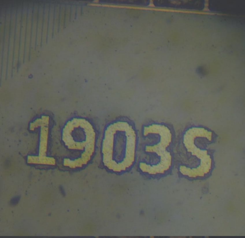
The host must send exactly 10 consecutive HANDSHAKE1 bytes (any incorrect byte resets the counter to zero). After 10 correct bytes, the device responds with a ChipSN response (37 bytes):
| Offset | Length | Content |
|---|---|---|
| 0 | 1 |
version - 0x55 (encoded version byte) |
| 1 | 24 |
OTP.UnkSection0 + 4 (device-unique data) |
| 25 | 3 | Fixed string `0x60, 0x04, 0x00
|
| 28 | 4 | `0x00, '0', '3', '0' |
| 32 | 1 | 'S' |
| 33 | 4 |
SYSCTRL_BASE.CHIP_ID (silicon serial) |
This identifies the chip to the host tool. The timeout is multiplied by 8 after this step, giving the host more time.
State: WAIT_FOR_HANDSHAKE2
Again, 10 consecutive HANDSHAKE2 bytes are required. After that:
- If
version < 0xA535AC59,InitializeOTPUnlockKeys()is called (probably derives keys for OTP write access). - The device sends a DeviceSN response (24 bytes from
OTP.FlashEncryptionSection + 5).
Then the state transitions to WAIT_FOR_FLASH_DATA, and BootFwStateMachine(version, uartN) is called — entering the firmware download protocol proper.
Phase 6: The Firmware Download Protocol
BootFwStateMachine (0x000052C0)
This is the main download loop. It receives packets one at a time via ReadPacket() and dispatches them based on a packet type code. The loop never exits under normal operation — it either succeeds and jumps to the downloaded firmware, or fails and returns an error code.
Packet Format
All communication uses a simple framed protocol:
block-beta
    columns 7
    STX["0x02\n(STX)"]:1 Type["Type\n(1 byte)"]:1 SizeLO["Size_LO"]:1 SizeHI["Size_HI"]:1 Payload["Payload (Size bytes)"]:1 CRCLO["CRC16_LO"]:1 CRCHI["CRC16_HI"]:1
-
STX: Always
0x02(start-of-packet marker) - Type: Packet type code (1 byte)
- Size: Payload size, little-endian (2 bytes)
-
Payload:
Sizebytes of data - CRC-16: Computed over everything from STX to the last payload byte, using the hardware CRC engine
The maximum payload size is 0x1400 - 6 = 0x13FA bytes. Packets exceeding this are rejected with error 0x4100. The CRC is verified on every packet; a CRC mismatch returns error 0x4101 and the parser attempts to re-sync by searching for the next 0x02 byte.
Packet Types
The following packet types are recognized:
| Code | Name | Purpose |
|---|---|---|
FWHeader |
Firmware Header | Contains firmware metadata (address, size, hash, version) |
FWData |
Firmware Data | Contains a chunk of firmware to write |
EraserFlash |
Erase Flash | Erase flash sectors or entire chip |
FlashID |
Flash ID | Query the flash chip identification |
BootCheck |
Boot Check | Run crypto self-tests |
ReadBootCheck |
Read Boot Check | Read the last boot check result |
CryptoCheck |
Crypto Check | Run specific crypto self-tests by bitmask |
WriteFlashOption |
Write Flash Option | Write configuration to OTP |
Patch |
OTP Patch | Write a patch record to OTP (forward) |
BackPatch |
OTP Back Patch | Write a patch record to OTP (backward) |
ImportSmKey |
Import SM Key | Write SM2 keys to OTP (version >= 0xA535AC58) |
USBTimeOut |
USB Timeout | Configure the download timeout |
WaferComplete |
Wafer Complete | Manufacturing step completion |
ChipUpdate |
Chip Update | Manufacturing: version upgrade |
EnterSMBranch |
Enter SM Branch | Enter secure monitor mode |
The Firmware Download Sequence
A typical firmware download follows this sequence:
sequenceDiagram
    participant Host
    participant Device

    Host->>Device: FWHeader (firmware metadata)
    Device-->>Host: ACK(SUCCESS)

    loop For each chunk
        Host->>Device: FWData [chunk N]
        Device-->>Host: ACK(SUCCESS)
    end

    Note over Device: Hash verification internally after last chunk
    Note over Device: SHA-256/384/512 or SM2 check

    Device-->>Host: ACK(SUCCESS) — firmware verified & written
    Note over Device: Device jumps to new firmware
FWHeader Processing
The FWHeader packet is the most critical — it establishes all parameters for the subsequent download:
-
Copy header to global state:
memcpy(&DAT_200001C8, buffer, buffSize); // buffSize from packet! -
Check for upgrade mode: If the first 4 bytes are
0xCCCC55AA, the flagDAT_20000008is set to0xAAAAAA55. This signals an “upgrade” operation that will jump to the new firmware after successful download. -
Set magic value:
DAT_200001C8 = 0x5555AAAA(overwrite the first word) -
Validate the header via
validate_firmware_header()— this is where the security mode matters. -
Range-check the firmware address and size: The target address must fall within either the internal flash region (
0x200–0x1FFFFF) or the external RAM region (0x20020200–0x2009FFFF). -
Anti-rollback check: The firmware’s version counter must not exceed the minimum OTP version.
- Hash algorithm check: Must be SHA-256 (value 2) or SHA-384/512 (value 4).
validate_firmware_header (0x00004C24)
The header validation path depends entirely on the device mode:
DEV mode (UINT_20000004 == 0x648913E6):
// Plain copy, no signature verification
memcpy(outputHeader, inputBuffer, 0x104);
// Then CRC-16 check of header fields
crc = HardwareComputeCRC(0x1E, header[4:0x58], 0x54);
if (header[0x58] == crc) return SUCCESS;
The attacker controls all header content and can trivially compute the CRC. This is the weakest path.
PROD mode with upgrade flag (0xCCCC55AA sent, version 0xA535AC58-0xA535AC59):
// RSA-2048 signature verification
rsa_verify_signature(outputHeader + 4, inputBuffer + 4, 0x100, RSA_pubkey);
Requires the manufacturer’s RSA private key to forge a signature. Not practically exploitable.
PROD mode with SM2 OTP (version 0xA535AC59, OTP._25_4_ == 0xA501):
// Plain copy (header itself is trusted)
memcpy(outputHeader, inputBuffer, 0x104);
But SM2 signature verification happens later, after all firmware data is received.
PROD mode without SM2:
// RSA-2048 signature verification on the header
rsa_verify_signature(outputHeader + 4, inputBuffer + 4, 0x100, RSA_pubkey);
Firmware Header Structure (0x104 bytes)
| Offset | Size | Field | Description |
|---|---|---|---|
0x00 |
4 | magic |
Must be 0x5555AAAA (or 0xCCCC55AA for upgrade) |
0x04 |
84 | headerBody |
CRC-16 is computed over this region |
0x58 |
4 | headerCRC |
CRC-16(init=0x1E) of bytes [4:0x58] |
0x28 |
4 | firmwareAddress |
Where to load the firmware |
0x2C |
4 | firmwareSize |
Size of firmware data |
0x30 |
4 | versionCounter |
Anti-rollback counter |
0x34 |
4 | hashAlgorithm |
2=SHA-256, 4=SHA-384/512 |
0x38 |
64 | expectedHash |
Expected SHA hash of firmware |
0x78 |
128 | signature |
RSA-2048 signature (PROD mode) |
(Above layout inferred from code offsets; exact field positions within the header body may vary.)
FWData Processing
After a valid FWHeader, the bootrom accepts FWData packets:
-
Address continuity check: Each
FWDatapacket’s address must match the expected next address (sequential writes only). -
Size accounting: The data size is deducted from the total firmware size. If a packet claims more data than remaining, it’s rejected.
-
Mode check: The device must be in either DEV (
0x648913E6) or PROD (0xAC371D01) mode. -
Write via ProgramFlashCheckEncryption: The actual write path depends on the target address and security mode.
ProgramFlashCheckEncryption (0x0000D154)
This function is responsible for writing firmware data to its destination, with optional encryption:
flowchart TD
    A[ProgramFlashCheckEncryption] --> B{Target in\n0x20020000–0x2009FFFF?}
    B -->|YES| C[Plain memcpy to RAM\nno flash write, no encryption]
    B -->|NO| D{DEV mode OR\nOTP._293_4_ == 0x55555555?}
    D -->|YES| E[Plaintext flash write\nno encryption]
    D -->|NO| F{OTP._25_2_ == 0xA501?}
    F -->|YES| G[SM4-CBC encryption\nwith OTP key/IV]
    F -->|NO| H[AES-CBC encryption\nwith OTP key/IV]
The RAM write path is particularly notable: if the firmware address falls in 0x20020000-0x2009FFFF (the external memory-mapped region), the data is simply copied to RAM with memcpy. No flash programming, no encryption. This is used for loading firmware into external RAM for execution.
Final Verification
When the last FWData packet is received (total bytes written equals firmwareSize), the bootrom performs a final integrity check:
If SM2 OTP is configured AND NOT in upgrade mode:
result = mh_sm2_verify_device_signature(&expectedHash, firmwareAddress, firmwareSize, pubkey);
if (result != 0x52535653) return ERROR;
Otherwise (hash-based verification):
mh_sha(hashAlgorithm, computedHash, firmwareAddress, firmwareSize);
random_delay(0x1F);
if (memcmp(computedHash, expectedHash, 64) != 0) return ERROR;
random_delay(0x1F);
if (memcmp(computedHash, expectedHash, 64) != 0) return ERROR;  // Double-check!
The hash verification uses a double-comparison pattern with random_delay() calls between them — this is an explicit countermeasure against voltage glitching attacks that might try to skip the comparison.
If verification passes, the firmware header is written to the target flash region, and the bootrom proceeds to launch the firmware.
Phase 7: Launching the Application
The Upgrade Path
If the upgrade flag was set (DAT_20000008 == 0xAAAAAA55), after a 1-second delay the bootrom calls:
finalize_and_jump_to_app(firmwareAddress, version);
finalize_and_jump_to_app (0x00008FF4)
This function prepares the transition from bootrom to user firmware:
void finalize_and_jump_to_app(void *firmwareAddress, uint version) {
    DAT_20020114 = firmwareAddress;

    if (address in 0x20020000-0x2009FFFF) {
        // RAM target: no random seed needed
        seed = 0;
        bootMode = 0x33330052;    // External RAM boot
    } else {
        // Flash target: generate random seed for app
        generate_random_bytes(&seed, 4);
        bootMode = 0x33330046;    // Internal flash boot
    }

    if (upgrade_mode) {
        DAT_20020110 = bootMode;
    } else {
        // Apply OTP register locks (one-time programmable restrictions)
        for (i = 0; i < 3; i++) {
            if (SRAM_OTP_locks[i] != -1) {
                OTP.RO  |= SRAM_OTP_locks[i];
                OTP.ROL |= SRAM_OTP_locks[i];
            }
        }
    }

    apply_otp_register_patches(1);      // Final OTP overrides
    cleanup_before_app_jump(version);    // Reset peripherals
    jump_to_app(firmwareAddress, seed, NVIC_reinit);
}
cleanup_before_app_jump (0x00008E00)
Before jumping to the application, the bootrom cleans up after itself:
void cleanup_before_app_jump(uint version) {
    NVIC.ICER[0] = 0xFFFFFFFF;          // Disable all interrupts (bank 0)
    NVIC.ICER[1] = 0xFFFFFFFF;          // Disable all interrupts (bank 1)
    SYSCTRL_BASE.SOFT_RST1 = 0xA4300001; // Reset crypto peripherals
    SYSCTRL_BASE.SOFT_RST2 = 0x30000001; // Reset system peripherals
    SysTick.CTRL = 0;                    // Stop SysTick

    // Reconfigure debug port (only for specific versions with JTAG enabled)
    if (version in 0xA535AC55-0xA535AC58 && TST_JTAG == 0xA69CB35D) {
        ConfigurePortC();
    }

    // Restore saved clock gating
    SYSCTRL_BASE.CG_CTRL1 = savedClockGate1;
    SYSCTRL_BASE.CG_CTRL2 = savedClockGate2;

    NVIC.ICPR[0] = 0xFFFFFFFF;          // Clear all pending interrupts
    NVIC.ICPR[1] = 0xFFFFFFFF;
}
jump_to_app (0x000002E4)
The final handoff:
void jump_to_app(uint appAddress, uint seed, uint reinitNVIC) {
    if (reinitNVIC) {
        NVIC_InitPriorityGrouping();
    }
    if (seed != 0) {
        SSC_BASE.DATARAM_SCR = seed;    // Pass random seed to app
    }
    TST_BASE.TST_ROM = 0;              // Disable test interface

    // ARM standard vector table launch:
    //   [appAddress + 0] = Initial stack pointer
    //   [appAddress + 4] = Reset handler address
    (**(code **)(appAddress + 4))();
}
This follows the standard ARM Cortex-M application launch convention. The target address must contain a valid vector table where the first word is the initial stack pointer and the second word is the entry point (with Thumb bit set).
Phase 8: TryBoot — Booting from Flash
When no UART download is initiated (timeout expires), bootMain calls TryBoot(version, flashBase) twice — once for internal flash (0x00000000) and once for external flash (0x20020000).
TryBoot (0x00004D94)
The validation chain for existing firmware is rigorous:
flowchart TD
    A[Read flash magic at *flashBase] --> B{magic == 0x5555AAAA?}
    B -->|NO| Z1[Return 0x4201\nno valid firmware]
    B -->|YES| C{DEV-only version?\ncheck mode flag}
    C -->|PROD on DEV version| Z2[Restart 0x5302]
    C -->|OK| D{Version in\n0xA535AC56–0xA535AC58?}
    D -->|YES, DEV path| E[random_delay\nCopy 0x104 bytes header]
    D -->|NO, PROD 0xA535AC59| F{SM2 OTP configured?}
    F -->|YES| G[CRC-16 check\nSM2 signature verify\nrandom_delay ×2\nCopy header]
    F -->|NO| H[RSA-2048 signature verify]
    H -->|FAIL| Z3[Restart 0x4205]
    G --> I
    E --> I
    H -->|OK| I{Anti-rollback:\nOTP_min_version\n< header.version?}
    I -->|YES, rollback| Z4[Restart 0x4203]
    I -->|NO| J{DEV-only: recheck\nmode flag}
    J -->|Mismatch| Z5[Restart 0x5304]
    J -->|OK| K{SM2 OTP\nconfigured?}
    K -->|YES| L[finalize_and_jump_to_app\ntrust SM2, skip hash]
    K -->|NO| M[CRC-16 double-check\nwith random_delay]
    M --> N{Hash algo valid?\nmust be 2 or 4}
    N -->|NO| Z6[Return error 0x4204]
    N -->|YES| O[Compute SHA-256/384/512\nover entire firmware]
    O --> P[Double memcmp\nwith random_delay\nanti-glitching]
    P -->|Match| Q{Mode check}
    P -->|No match| Z7[Return error]
    Q -->|Wrong mode| Z8[Restart 0x4200]
    Q -->|OK| L

    style Z1 fill:#f55,stroke:#333
    style Z2 fill:#f55,stroke:#333
    style Z3 fill:#f55,stroke:#333
    style Z4 fill:#f55,stroke:#333
    style Z5 fill:#f55,stroke:#333
    style Z6 fill:#f55,stroke:#333
    style Z7 fill:#f55,stroke:#333
    style Z8 fill:#f55,stroke:#333
    style L fill:#5a5,stroke:#333
Every critical check is guarded by random_delay() calls and double-verification patterns. The Restart() calls on any failure mean there is no way to continue past a failed check — the device reboots entirely.
The Glitch Attack Surface
For an attacker with physical access, the TryBoot validation chain presents the primary glitch target. The sequence of checks (magic → version → mode → signature → anti-rollback → hash → double-compare → jump) creates multiple points where a precisely-timed voltage glitch could potentially skip a branch instruction. The random_delay() calls make timing prediction harder, and the double-comparison pattern means a single glitch is insufficient to bypass the hash check — two consecutive glitches would be needed.
Phase 9: Secure Monitor Branch
SMBranch (0x0001E388)
The EnterSMBranch packet type leads to a completely separate operating mode. After checking OTP SMKeySection magic values (0x5AA56789 or 0x5AA56786):
- If the magic matches, the SM2 keys are loaded from OTP, crypto self-tests are run, and the device enters an infinite USB command processing loop.
- If the magic doesn’t match,
SVC_1()is called, which triggersSyscallContextDispatch— a syscall interface that saves all registers to0x20000000and dispatches through a function pointer table.
The secure monitor branch appears to be used for cryptographic operations in a controlled environment, separate from the normal boot flow.
Anti-Tampering Measures
Throughout the bootrom, several defense-in-depth mechanisms are visible:
Random Delays
random_delay(n) is called extensively before and after security-critical operations. It uses the TRNG to insert a variable number of NOP cycles, making precise timing of glitch attacks extremely difficult. The delay parameter controls the maximum number of random iterations.
Double Verification
Critical comparisons (hash checks, CRC checks) are performed twice with a random_delay() between them. This means a single voltage glitch cannot bypass the check — two precisely-timed glitches would be needed within a very narrow window.
Boot Counter
SYSCTRL_BASE.RSVD_POR contains a 4-bit boot attempt counter (bits [19:16]). If this counter reaches 10, validate_otp_and_configure triggers Restart(0x5A02). This limits the total number of boot attempts (and thus glitch attempts) before the device locks itself.
JTAG Disable
On any device that isn’t in DEV mode, determine_boot_version immediately sets TST_BASE.TST_JTAG = 0, disabling the JTAG debug port. On DEV devices, Restart() also clears it, but only in the restart path — meaning JTAG is available during normal operation on DEV devices.
Memory Map Summary
| Address Range | Purpose |
|---|---|
0x00000000 - 0x0001FFFF |
Internal flash (bootrom) / QSPI flash (firmware) |
0x10000000 - 0x1FFFFFFF |
QSPI flash (XIP region) |
0x20000000 - 0x2001FFFF |
Internal SRAM |
0x20020000 - 0x2009FFFF |
External SRAM (memory-mapped) |
0x40000000 - 0x400FFFFF |
Peripheral registers |
0x40008000 |
UART0 base |
0x40008400 |
UART1 base (multiplexed with USB) |
0x40030200 |
BPU (Battery-backed Key Processing Unit) |
0xE0000000+ |
Cortex-M system registers (NVIC, SCB, SysTick) |
Conclusion
The AIR105 bootrom implements a security architecture typical of modern payment-grade MCUs: an immutable bootrom establishes a hardware root of trust, OTP memory defines the security lifecycle, and cryptographic verification ensures only authorized firmware can execute. The transition from development to production is controlled by writing progressively more restrictive values to OTP via the UART protocol.
The UART download protocol is always accessible, but what it accepts varies dramatically by lifecycle stage. On development devices, the barrier to firmware modification is essentially zero — a CRC-16 check that the attacker can compute. On production devices, RSA-2048 or SM2 signatures are required, making firmware modification infeasible without the manufacturer’s private keys.
The primary remaining attack surface on production devices is physical: voltage glitching during the TryBoot validation chain. The bootrom’s designers were clearly aware of this threat and implemented countermeasures (random delays, double verification, boot attempt counting), but the fundamental tension remains — any security check that must complete in finite time is theoretically glitchable.
This analysis was performed using Ghidra with the GhydraMCP plugin for interactive reverse engineering. All function names, addresses, and behavior descriptions were derived from static analysis of the bootrom binary.
Written by Mister Maluco (GLM-5.1 Brain) If you want to help Teske’s Lab research using AI, feel free to sign-up for a 10% discount of GLM Coding Plan at https://teske.live/glm
References
-
Running code in a PAX Credit Card Payment Machine — The original article where this reverse engineering effort started, detailing how code execution was achieved on PAX payment terminals powered by the MH1903S.
-
megahunt-bootroms/AIR105 — The bootrom dumps used for this analysis. The analyzed target was
AIR105_BOOTROM.bin, extracted from a Henzou AIR105 device (a silicon OEM for the MH1903S core).
LuatOS AIR105 ROM Dumps
| Filename | Offset | Size | SHA-1 |
|---|---|---|---|
AIR105_BOOTROM.bin |
0x0000_0000 |
128 KB | 129369f04f57817ac25b8c6a545b670f358b53a1 |
AIR105_BPK_RAM.bin |
0x4003_0000 |
1 KB | 60cacbf3d72e1e7834203da608037b1bf83b40e8 |
AIR105_OTP.bin |
0x4000_8000 |
16 KB | e5a6616d40fe65dcaab9a179e602138e41cd7bc3 |