Running code in a PAX Credit Card Payment Machine (part1)
 Written by
Lucas Teske
Written by
Lucas Teske
on
Disclaimer
All procedures described here were done with public available stuff - No security flaws were actually explored here to get code execution. The processor swap technique does not bypass the tamper protections neither allow a fake machine to actually emit payments.
Brazilian credit card payment machines usually are in state of the art regarding security measures. I remember once a Elavon employee told me that Brazil got all the first releases of payment machines and systems. When asked why, he said: frauds in Brazil are sophisticated enough, that if the system is secure enough to Brazil, it works for anywhere in the world.
In the future, I will make an article about the security measures that both, MegaHunt, PAX and Brazilian companies implement in their machines to avoid systems to be tampered with.
If you’re sharing / commenting over this article, please put the same disclaimer there. I don’t mind using information here to make new articles, but Brazil suffers a lot with fake news (specially involving security hardware made here) and someone can think that makes it possible to hack their credit cards or accounts (you know, people lacking the knowledge to actually understand whats involved).
Head Notes
This article is sort of incomplete. I will still publish the reverse engineering of the boot rom and how I created an emulator to better map out what the firmares do. Here I just mention briefly that I did an emulator and I think that deserves its own article. I will update this head note when they’re published.
I want to thank Gutem and Penegui for a quick technical review of the tech content of the article, and Pag, which gave a really fast and friendly response when I sent to them. A short timeline is provided at bottom of this page.
Credit card payment machines
Here in Brazil, there are several companies that act as payment gateways and these sort of stuff. I would guess the biggest ones are PagSeguro and MercadoPago. While PagSeguro is originally from Brazil, MercadoPago is from Argentina and came from a completely different business (MercadoLivre, which is basically the south american equivalent of eBay).
There are also lots of banks that also has payment machines nowadays, but I would guess most of them, if not all, buy the machines from a Brazilian manufacturer called TecToy (which was previously done only by Transire, but now they’re merged into the same company).
I find it funny, because TecToy is a toy maker, but they are huge and old and basically one of the few surviving companies that actually make hardware in Brazil. Nonetheless to say, the machines are not designed by them, but most by Chinese OEM. Mostly nowadays, its either PAX or Sunmi.
In Brazil, its very easy and cheap to buy them basically anywhere, easiest ones are from the companies I described above (Pag and MP). For example, for PagSeguro, you can find them in their website.
Just for a reference, by the time I wrote this article, US$1 ~ R$5,48 so most of these machines are under US$20, which is cheap even for Brazilian standards by the hardware they posses.
Mercado pago is a bit more expensive, but easier to buy since you can just go to their normal market place (Mercado Livre) which is like EBay and buy the machines (see https://lista.mercadolivre.com.br/maquina-de-cart%C3%A3o#D[A:Maquina%20de%20Cart%C3%A3o] )
In short: they are usually PAX based machines, with same “Operating System” but custom application which are totally different beast between then. Additionally, Pag also does “Merchant OEM” and lots of payment companies that offer machines actually use a unbranded Pag machine and use their API for doing all the stuff (so for any Brazilians reading this, if you buy a machine that’s not from MP or Pag, chances are, its from Pag anyways).
For sake of simplicity, these machines correspond to these PAX ones:
- Mini Chip 3 - PAX D188 (Baremetal)
- Moder Plus 2 - PAX D195 (Linux OS)
- Moder Pro 2 - PAX Q92S (Linux OS)
- Mini NFC 2 - PAX D177 (Baremetal)
- Mini Smart 2 - Sunmi P2 (Android)
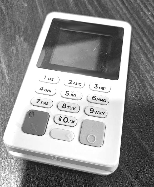
For this article, I decided to use the Mini NFC 2, which is a simple and cheap PAX D177. Worth notice, that even though the Chip 3 (D188) looks way more advanced, it has basically the same hardware as D177, but an additional LTE Modem and a bigger screen. Firmware that runs on both are basically the same.
First works and Identifying stuff
So usually for reversing secure hardware, I buy at least three machines when possible. Usually it goes like:
- Will open, let every single protection trip on it
- Will use to try bypass protections (if needed to my objective)
- Will keep as is, for comparing with a working machine.
In that specific scenario, I just wanted to run DOOM on them, just because, if it computes, it needs DOOM.
I had previous experience reverse engineering these machines, so most of the article is just an example how I would do it (for this article, it actually took me few years to get to the current state) and how I remember I did. So I was expecting:
- Heavy security
- Tamper protection
- Clock Glitching protection
- RNG Manipulation protection
- Code signatures
- Code encryption
- Lots of frustration
I could go into two ways for code running: Exploiting it, swapping CPU. For exploiting it, I would need to find a flaw that allowed to execute code through Bluetooth, Smartcard, NFC or USB. These are the only interfaces. For that, I would need to have the entire code, and as we will see, that was sort of not possible.
Second way, would be to get whatever CPU was in the board, remove it and install a new and unfused one. The problem with that, is to actually find the CPU to sell anywhere.
So either way, I would need to open the machine and identify stuff. Just for the reference, the machine was this one:
On the back side, there are few screws which are easily removed. I usually do this with the machine turned on. So I can see which actions would trigger the tamper protection.
 Removing the screws does not trigger the tamper protection, but removing the case does. In the picture below, you can see the case removed, and I highlighted two of the tamper detection points.
 on the back side of the case, there is some carbon-rubber points that touch these tamper points in the PCB. It works exactly the same as video game consoles controller buttons, but in this case, they just ensure the “button is always pressed”.
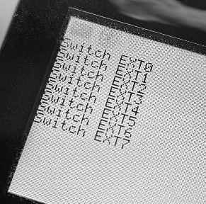
And for some reason, the machine decided to tell us which one of the tampers we triggered :)
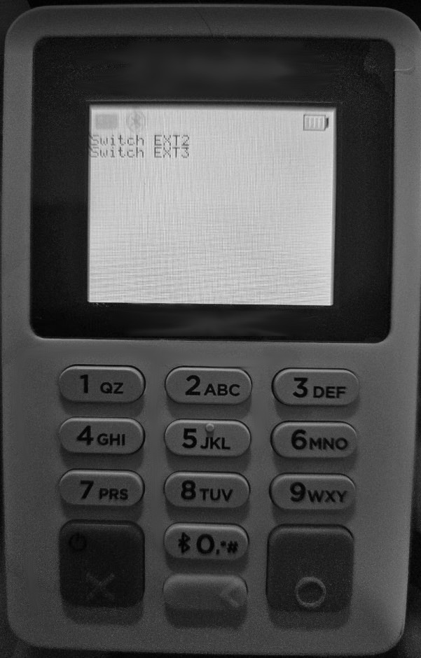 Also this resets over boot, do if you bridge them, you can use it to identify the names of each tamper point hehe.
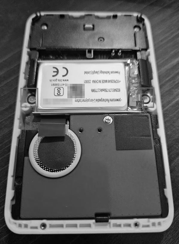
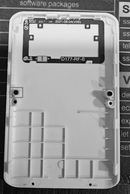
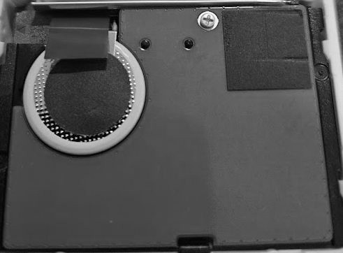
So in this bottom part, we can see some stuff. There is the round coin cell battery in the left, and there is a big boring green PCB. They’re basically over the card reader and all the core circuits.
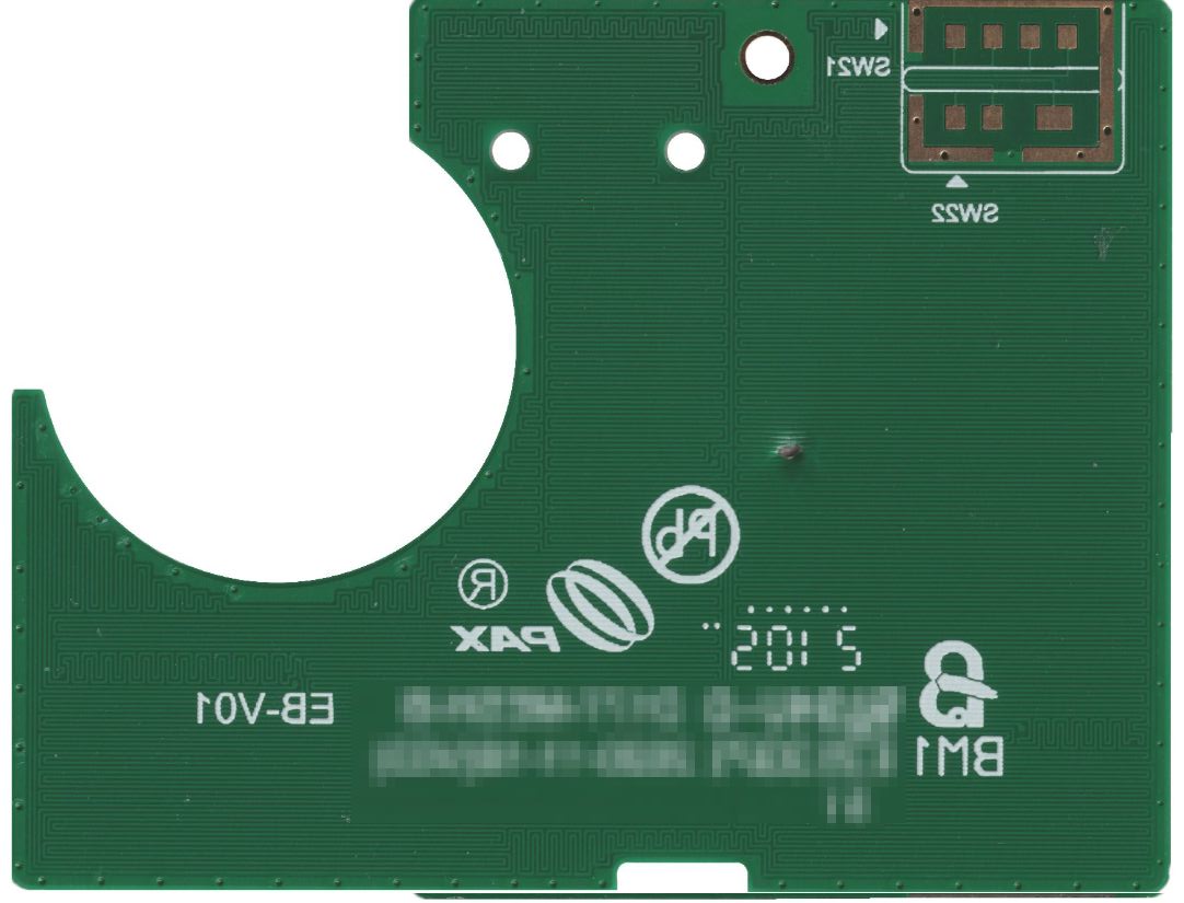
Although this PCB looks boring, don’t get fooled by it. That’s basically a 4 layer PCB with a DENSE mesh inside it. Any damage or removal will trigger another tamper point. Just for quick reference, this is a scan of the PCB:
Removing all the plastic stuff, we reach the main PCB:
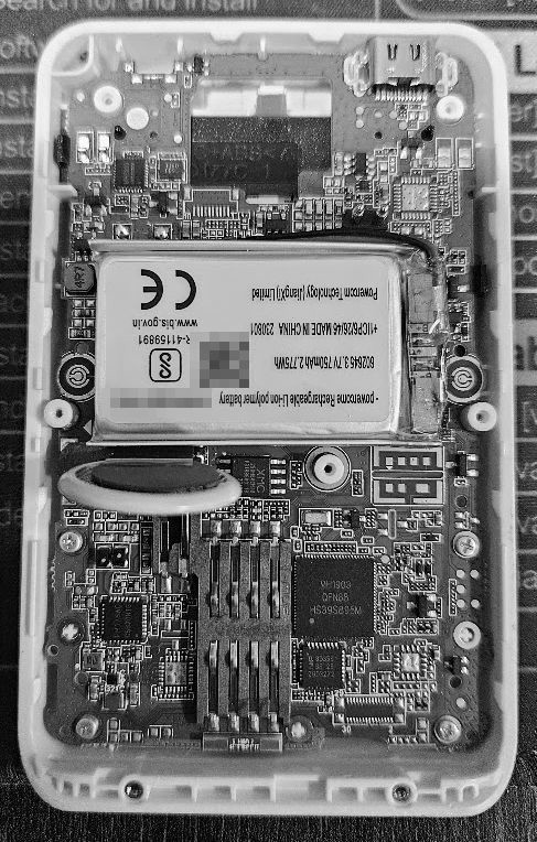
There is lot of stuff, but the stuff that we care in the bottom.
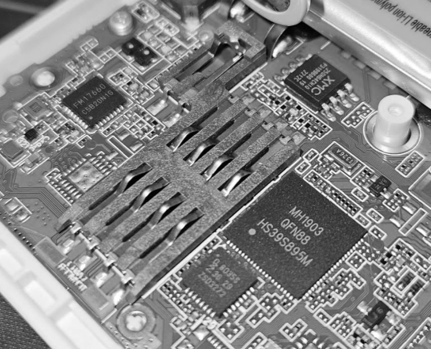
Here we can see some interesting stuff:
- MH1903 - Our main SoC (CPU)
- NXP 8035S - Smartcard Interface PHY
- FM17660 - NFC Reader
- XM25Q65 - 16MB SPI Flash Memory
(And as you guessed, we trigger about every tamper point in the back)
The flash memory, we can dump it. I have both tampered and untampered dumps from it. Bypassing tamper is left as exercise for the reader :). But if you just want to understand how it works, you can just dump as is, since the tamper doesn’t actually erase the entire flash, but just some parameters for communicating with the payment servers.
I was expecting always that the flash would be encrypted, but it isn’t. Still, we can’t change its contents since its signed (everything is signed basically) so we can use it for reverse engineering but not for code execution. But its neat that it is a 16MB flash, so it fits a entire DOOM WAD file :D
What we know about MH1903
So here is where things get REALLY annoying. This SoC is actually behind a curtain of obscurity. The core is done by MegaHunt, which only provides this as information:
 (see https://www.megahuntmicro.com/en/index.php?catid=5 )
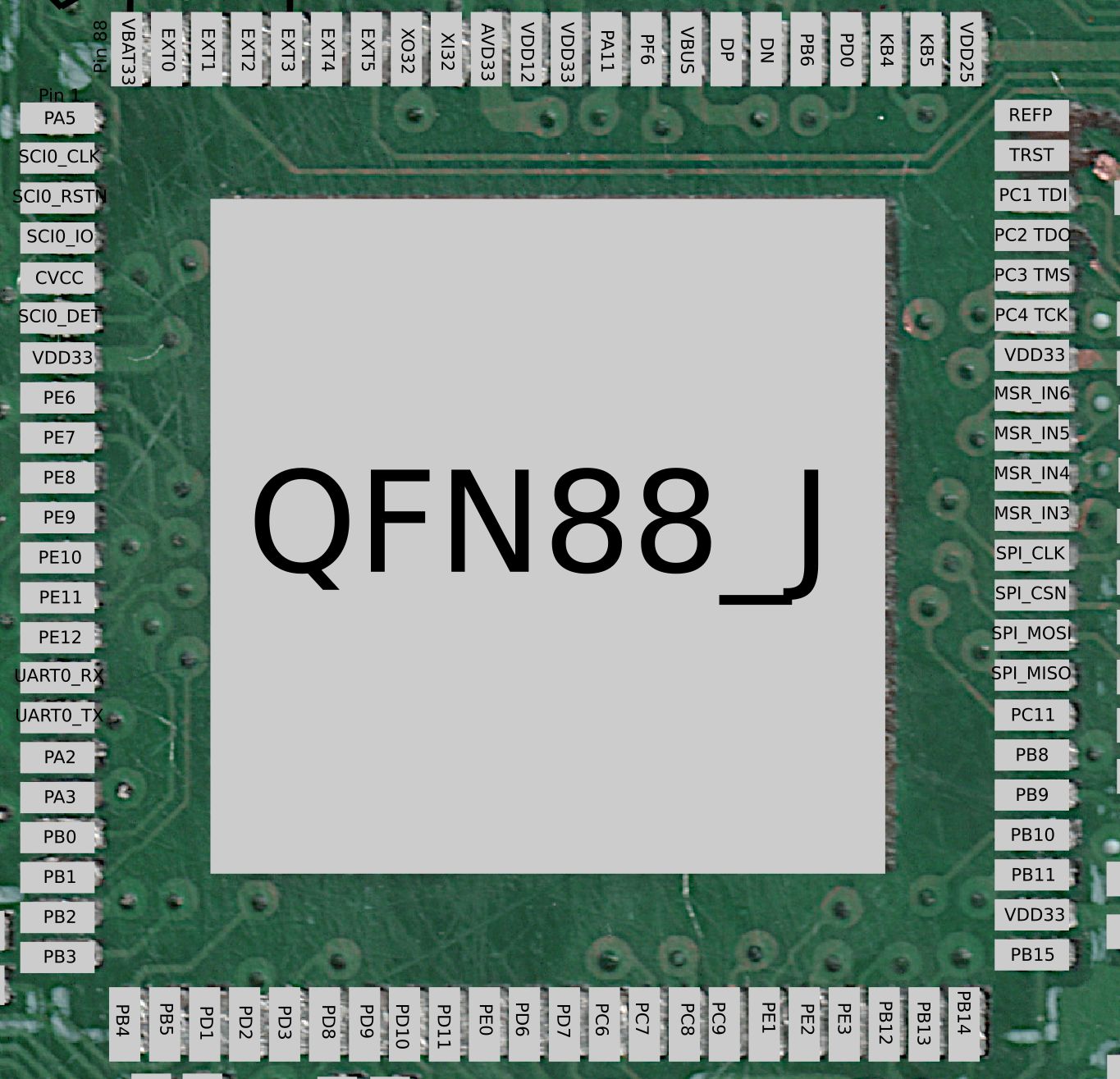
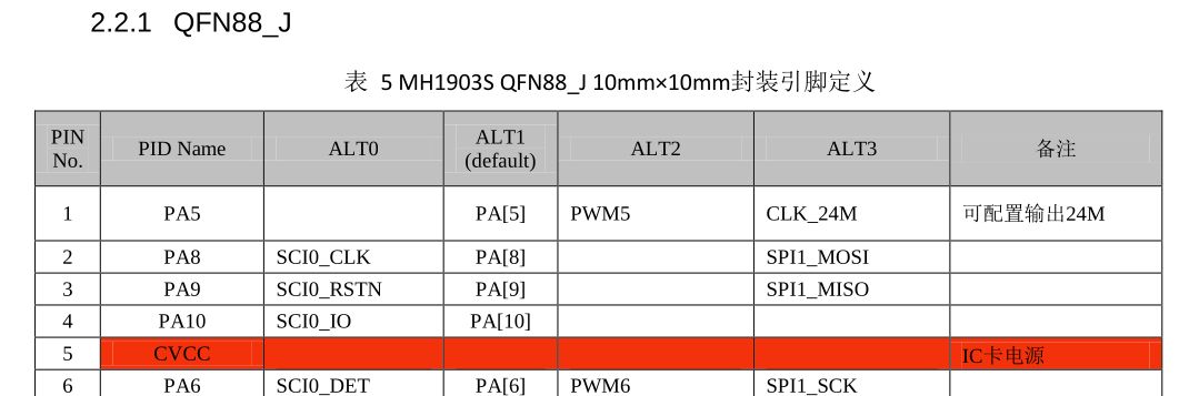
Digging it a bit deeper in google, we can find few suppliers that has more info. It has lots of variants, but in short their core is the same, just changing exposed pins and/or flash/ram inside the SoC. That specific one, is the QFN88 version which has the following specs:
- RAM: 1MB
- FLASH: 1MB
- SPI: 4
- ADC: 5
- DAC: 1
- GPIO: 64
- USB: 1
- Serial: 4
As you can see, there is an internal flash which is a pity for me. I’m still building my gear to be able to probe directly to the flash. I already did some decaps, and the flash isn’t embedded in the main silicon, but just glued over the main die and bound wired to it. I heard from some people from semiconductor industry that this is because its very hard to do flash and CPU in the same process, at least with decent enough density, so its usually preferable (and cheaper) to make them separated.
One thing worth noticing though, the BGA versions does not have embedded flash, so their program are loaded from external flashes. Spoiler alert: the D188 has two flash memories onboard :)
Also there is the MH1903S variant with has a beefy spec on flash but less RAM and less GPIO / SPI
- RAM: 640KB
- FLASH: 4MB
- SPI: 3
- ADC: 6
- DAC: 1
- GPIO: 56
- USB: 1
- Serial: 3
So google didn’t had much information, although I did found some SDKs around github (mostly mirrored from chinese git) and I had to search in Baidu. So this part took a very long time, since lots of information are not available outside mainland china, and since there is several variants of MH1903, I got several datasheets with conflicting information. Also most of them I had to pay for accessing it on CSDN, which luckily there are some brokers that does that for you. In the foot of this page there is a note with a link to all datasheets I could find so if you ever need, there is there. Just be warned: lots of conflicted info and it seens some wrong and omitted stuff is everywhere.
So how did I test my assumptions? Well, I found by a chance that there is a arduino like chinese board from LUAT that uses an SoC called AIR105, it seens boring, but some of my baidu search pointed out that AIR105 actually uses a MH1903S core. The AIR105 are also available in aliexpress very easily to buy: https://s.click.aliexpress.com/e/_oBLNTrc
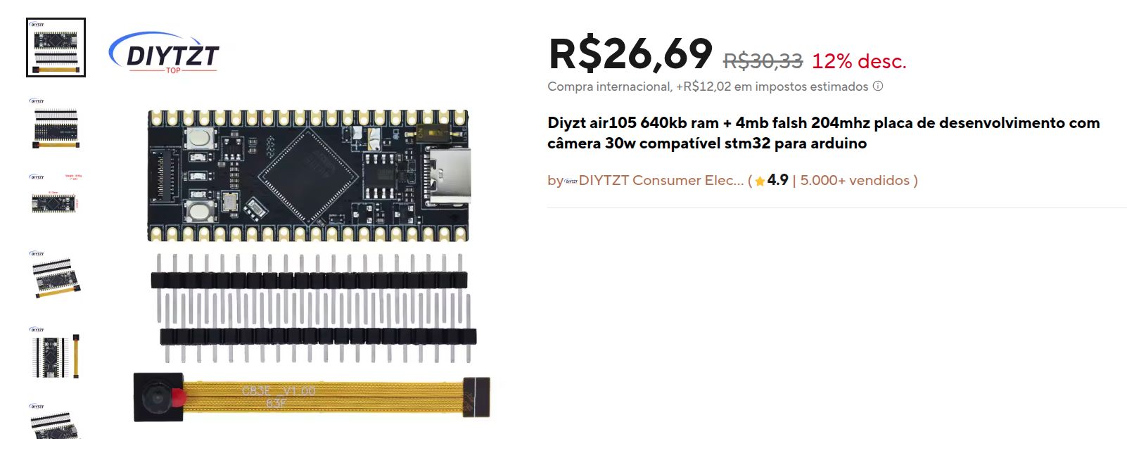
I bought a few, decaped one and guess what. it is indeed a MH1903S :D
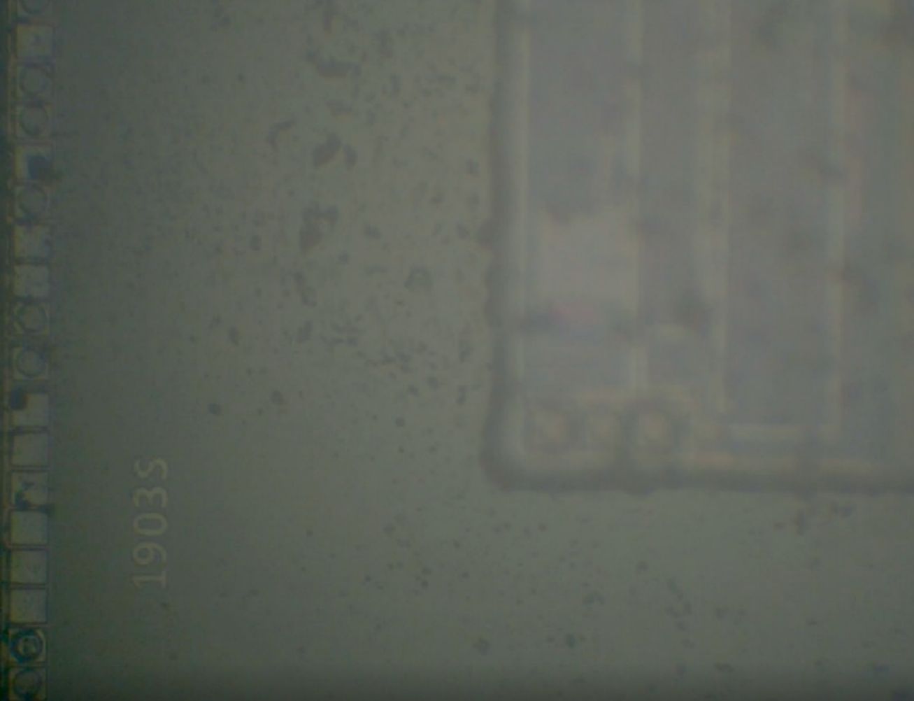
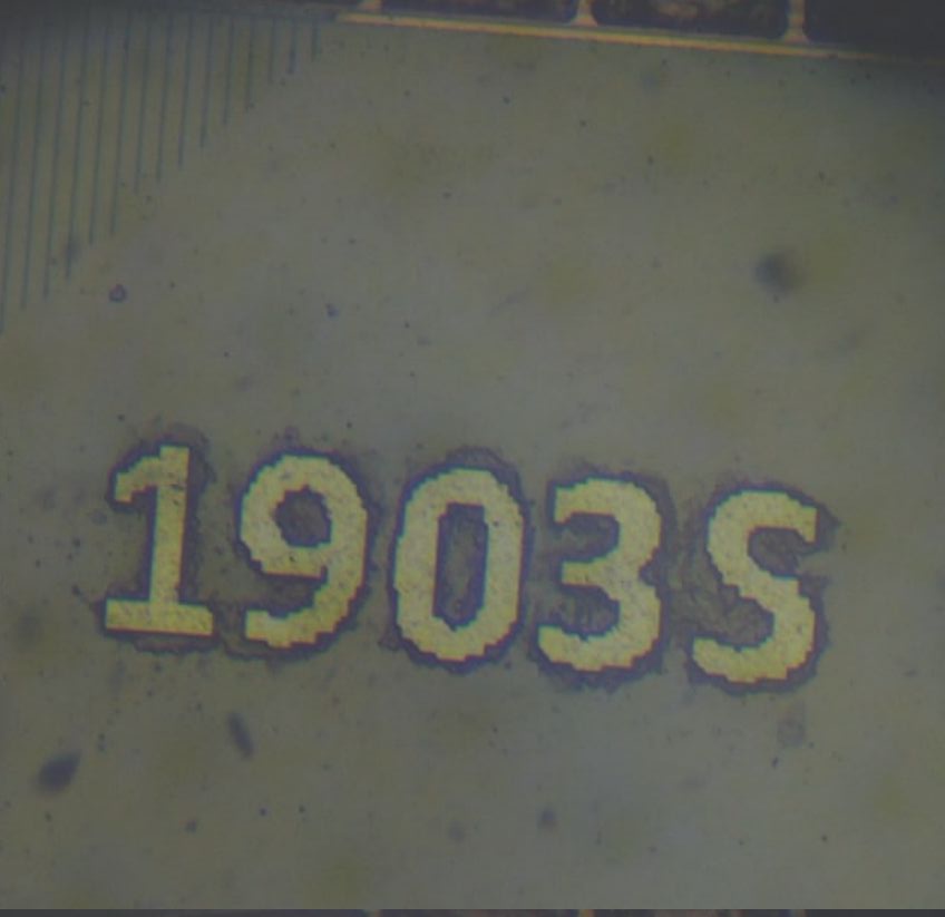 As a reference, when I decaped one of t he SoC from the machine, the writing was 1903A:
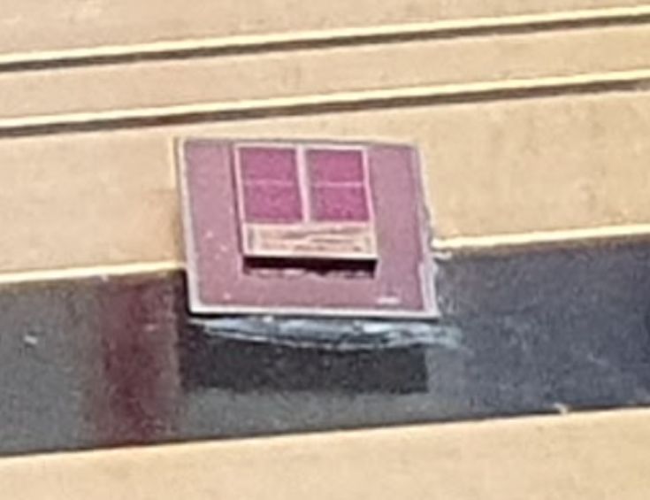
 Also, remember when I said flash memory is glued over the main die? Here is a shot showing both of them (sorry, I didn’t made a focus stacking). Flash memory is the one out of focus in the right. Bound wires are dead because I used 78% Nitric Acid and they’re copper ones.
 So basically, we could assume they’re similar at least. Their datasheets also tell about the same thing (seems like the only different is actually flash + ram)
The block diagram for this CPU is described in datasheet, and this is basically the only info that matches across all datasheets I’ve found:
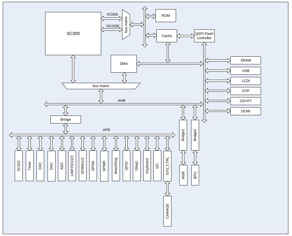
So SC300 is actually a ARM spec called SecurCore. Its a Cortex M3 (in case of MH190x is a M4F) with some security enhancements. For example, although they’re 32 bit simple ARMs, they have security boundaries between OS <> App which are configured in memory controller registers (primitive version of TrustZone). It also follows some standards that are only available under NDA, and I can only guess what they’re. Just for quick reference: The CPUs inside your credit cards, follow the exact same specification.
Datasheets also specifies some memory maps, which at least all datasheets agree, although its clearly not everything the device has. For example, MH claims that CPU has hardware acceleration for RSA, AES, hashes and stuff, but there is nothing in memory map of the datasheet. I found out later, that they’re just being obscure or require a NDA to that. I will eventually map everything by reverse engineering apps I dumped and some SDK with binaries I found over the internet. Also please let me know if these addresses matches any target arch you actually played with. I couldnt find anything, so it seens not a direct clone of any existing SoC in the market (I speculated a STM32 or ATSAMD but they dont match).
| Address Range | Peripheral name | Bus Name |
|---|---|---|
| 0x4000_0000-0x4000_03FF | SSC | AHB |
| 0x4000_0800-0x4000_0BFF | DMA | AHB |
| 0x4000_0C00-0x4000_0FFF | USB | AHB |
| 0x4000_1000-0x4000_13FF | LCD | AHB |
| 0x4000_8000-0x4000_BFFF | OTP | AHB |
| 0x4006_0000-0x4006_FFFF | DCMI | AHB |
| 0x4008_0000-0x4008_FFFF | CACHE | AHB |
| 0x400A_2000-0x400A_2FFF | QSPI | AHB |
| 0x400A_3000-0x400A_3FFF | SPIM5 | AHB |
| 0x4001_0000-0x4001_0FFF | SCI0 | APB0 |
| 0x4001_2000-0x4001_2FFF | CRC | APB0 |
| 0x4001_3000-0x4001_3FFF | Timer0 | APB0 |
| 0x4001_4000-0x4001_4FFF | ADC | APB0 |
| 0x4001_5000-0x4001_5FFF | SCI2 | APB0 |
| 0x4001_6000-0x4001_6FFF | UART0 | APB0 |
| 0x4001_7000-0x4001_7FFF | UART1 | APB0 |
| 0x4001_8000-0x4001_8FFF | SPIM1 | APB0 |
| 0x4001_9000-0x4001_9FFF | SPIM2 | APB0 |
| 0x4001_A000-0x4001_AFFF | SPIM0 | APB0 |
| 0x4001_B000-0x4001_BFFF | SPIS0 | APB0 |
| 0x4001_C000-0x4001_CFFF | Watchdog | APB0 |
| 0x4001_D000-0x4001_DFFF | GPIO | APB0 |
| 0x4001_E000-0x4001_EFFF | TRNG | APB0 |
| 0x4001_F000-0x4001_FFFF | SYS_CTRL | APB0 |
| 0x4002_0000-0x4002_FFFF | MSR | APB1 |
| 0x4003_0000-0x4003_7FFF | BPU | APB2 |
| 0x4004_4000-0x4004_4FFF | UART2 | APB3 |
| 0x4004_5000-0x4004_5FFF | UART3 | APB3 |
| 0x4004_8000-0x4004_8FFF | KEYBOARD | APB3 |
| 0x4004_9000-0x4004_9FFF | I2C0 | APB3 |
RAM is mapped in the usual place for most of these ARM Cortex chips. They’re based on 0x2000_0000, and span up to the max size (640KB for MH1903S and 1MB for MH1903). The bit bands are also in the places we expected, being 0x2200_0000 for the SRAM. There are also more devices there, that I didn’t wrote here. These will have their own article after I finish mapping it everything I can.
The main MH1903S datasheet shows two variants of the QFN88, one having a _J suffix. The non J has a internal 3.3V regulator which is very handy for boards like the AIR105. By reverse engineering the D177 machine board, it seems like the pin-out almost exactly matches the J variant. We will see later, that I had a hard time because I assumed that the datasheet would be correct.
Finding out how things are wired
So first thing, I need to figure out at least where the UART is wired (if wired). I know the USB is wired to the hardware USB (since pins are fixed) but for some reason, I don’t see the boot rom up in the USB so I must find the direct UART.
UART pins are usually exposed for diagnostics during manufacturing, either that or JTAG. JTAG (or more specific here, SWD) in case of this device is disabled during boot, so I decided to not waste much time finding it in the board.
So how to start finding things on the board? Well I usually like to remove all components from the board and make a nice scan of it (using normal paper scanners). Then I overlay the pinout of the CPU and “trace back”. A nice application to do that is Inkscape. It allows you to draw stuff vector based, and scanned images has 1:1 size match with real world (in case you need measurements).
Then I draw the pads as gray rectangles, name them:
 I usually like to mark vias as well, since these boards are multilayred and you probably will need it to fully follow the tracks:
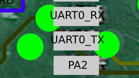 For example this TX/RX tracks passes through the front of the PCB as well (don’t mind the misalignment, not sure why the image currently is like that)
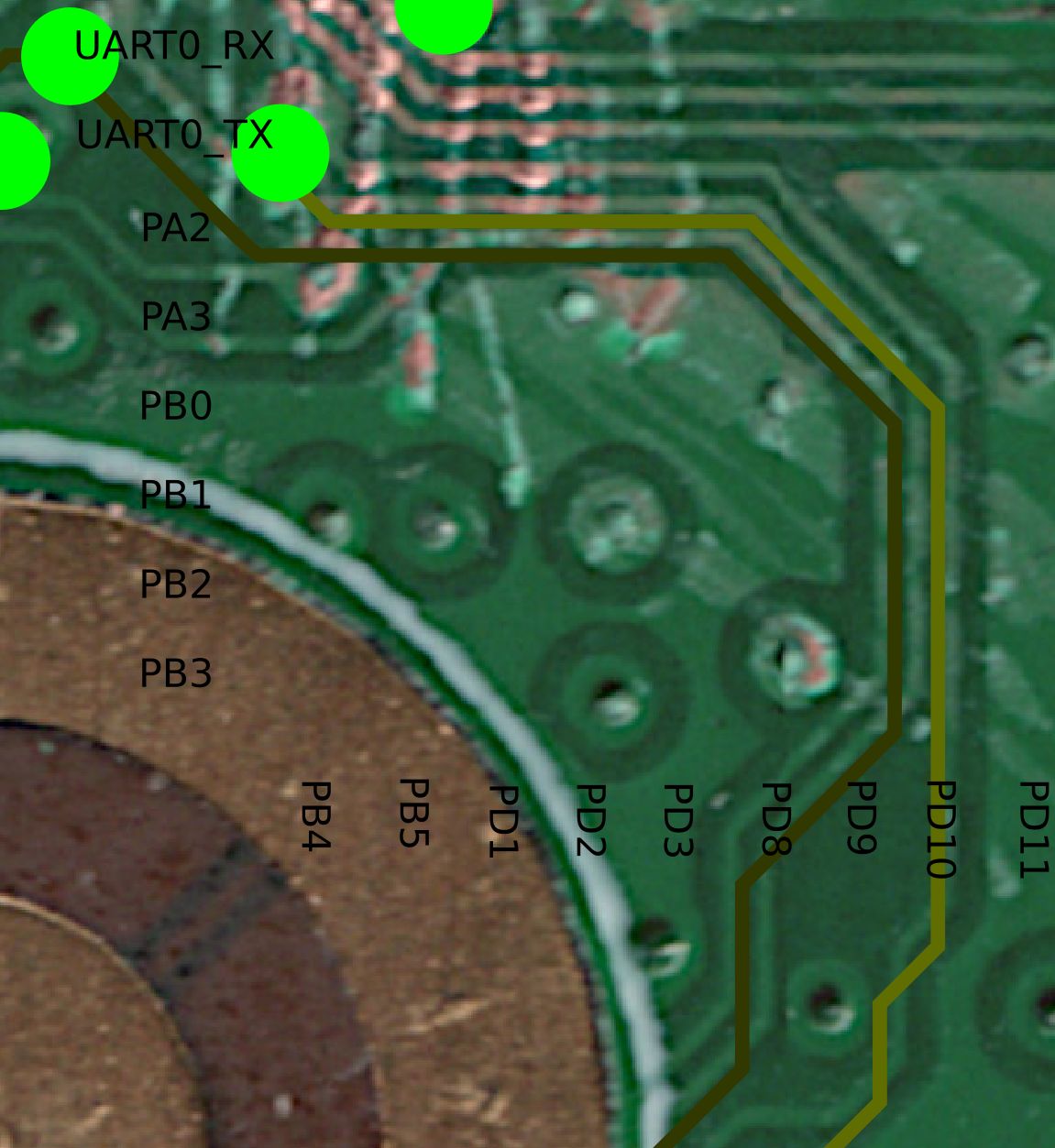 After following it through, I reached 2 of the 5 test pads in the right corner of the backside of the PCB, which I also marked in inkscape.
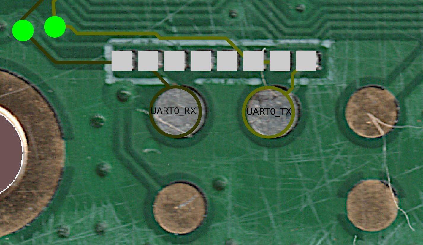 So now that I had the UART, I could use it to reprogram the machine after a CPU Swap.
And for those who are wondering: this UART, application wise, is the same as the USB port and Bluetooth so no leaky stuff (usually) is there, but the same thing the mobile application acesses it. And if it does, you don’t actually need to open it, since Bluetooth / USB will leak it the same.
So now that I had the UART, I could use it to reprogram the machine after a CPU Swap.
And for those who are wondering: this UART, application wise, is the same as the USB port and Bluetooth so no leaky stuff (usually) is there, but the same thing the mobile application acesses it. And if it does, you don’t actually need to open it, since Bluetooth / USB will leak it the same.
CPU Swap
So one of the easiest ways I could get code running and skip requiring bypassing the secure boot of the MH devices is by just getting the CPU and swap. Some might consider this a vulnerability, although I personally don’t consider it: Even if someone gets hand in the entire code for the machines, there are still the keys and data loaded into the NVRAM which are used for the card transactions. I already saw some cases few years ago that the keys were actually stored inside the flash memory (so if you nuke the CPU before the tamper detect, you retain everything). That’s not the case of these machines.
Sadly these MH1903 devices are pretty rare to buy outside mainland china. From time to time they appear in Aliexpress as well. Here is an affiliate link: https://s.click.aliexpress.com/e/_oBMot6n although it might be dead when you check this out (since they’re pretty rare).
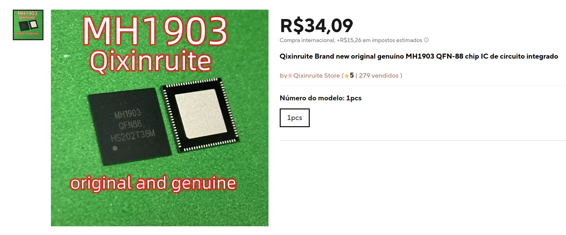
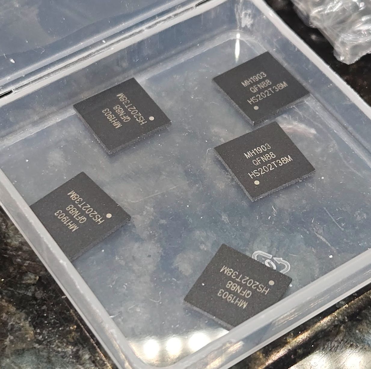
So its a bit expensive, R$34 (CPU) + R$15 (TAX) per device, plus R$28 shipping. I bought 5 of them just in case which was about R$150 (US$28) with the shipping.
 Few years ago I tried swapping the CPU in that machine without any success. So I thought the issue was that the variant I had wasnt the J but the same as AIR105 (which would sort of make sense) and that made me sad. But I decided to try swap one of the AIR105 for that one just to dump the bootloader (more bootloaders = more info)
After trying to that, I noticed the board was fully dead. No power besides the +5V. After swapping two boards I remember something I saw in the datasheet:
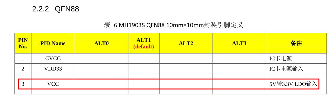 One of the differences between the J and non J version, is that the non J version (in this case AIR105) had an internal 3.3V LDO. And checking the schematics of the AIR105 board, guess what? No regulator onboard, everything was powered from the LDO.
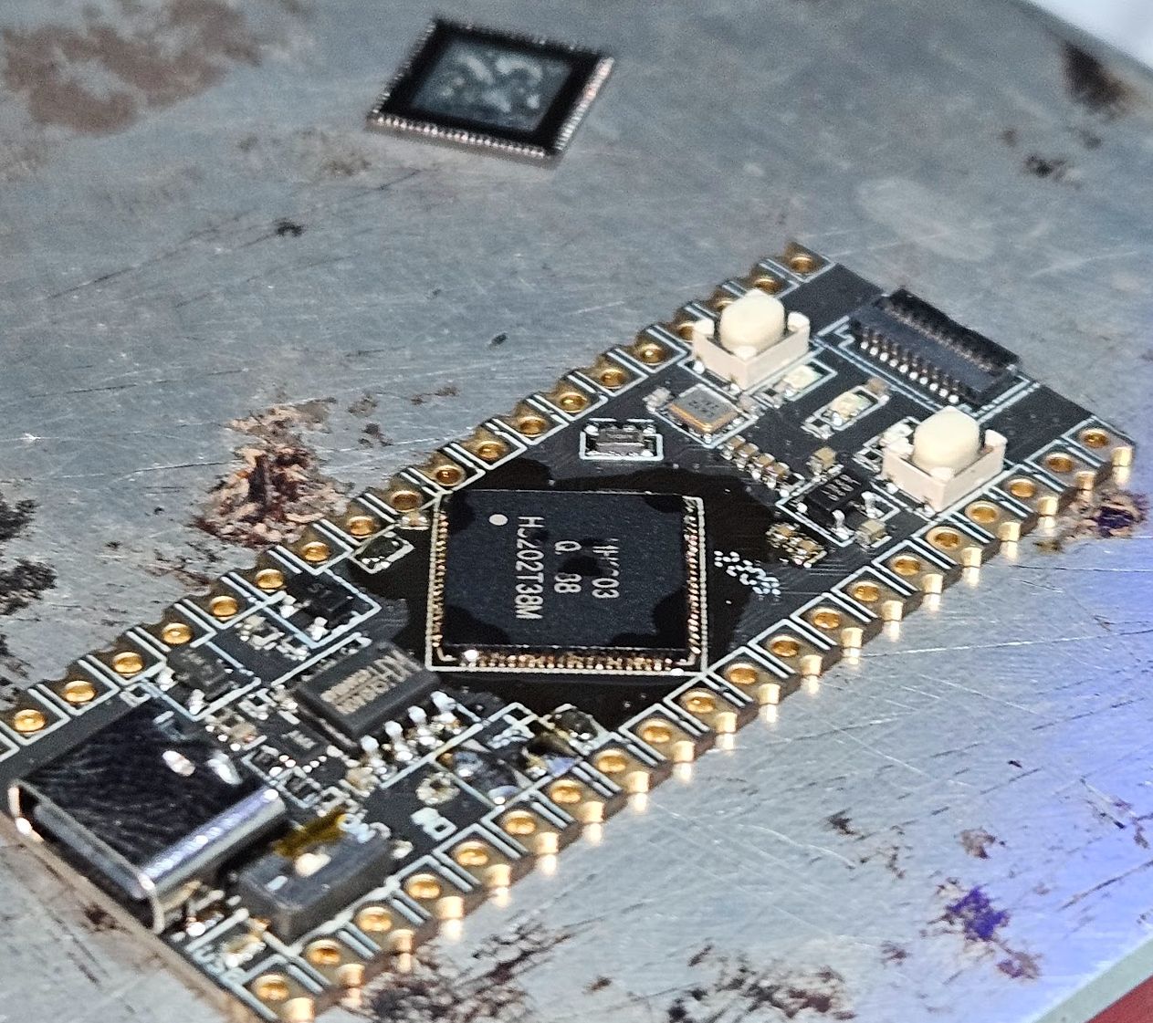
So it would make sense that the board doesn’t have any power at 3.3V, since the J version does not have it. So I decided to give another try swapping the CPU on the D177 board. For that, I decided a fully fresh start: new machine with the box just open and a not used MH1903 CPU. The result? Nothing from the board. Not on UART, not on USB (and there should be both activity).
Basically what happened is that, the boot rom never answered to handshake calls, which was odd. So I decided to give a try on the AIR105 board, just to notice that the board actually had to be reset by toggling the RTS signal in the serial port.
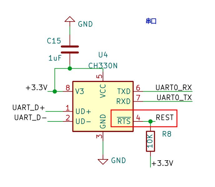 So that made me wonder: How was it resetting the board? By looking at the pin-out, there is no reset button. But looking at AIR105 board schematic, we see a interesting thing:
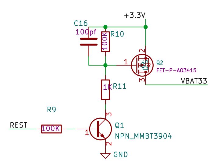
Basically, the board didn’t had any coin-cell battery where it should, just a capacitor for emulating the board (the XH311H battery in the schematic, is just a not populated connector in the board), and what the reset pin actually did, was to short it out the power supply at that pin, making it 0V. And guess what? The datasheet told me all the time, but my lack of Chinese reading skills just bypassed it 😆
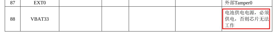 For those (like me) which is very rusty in Chinese, the marked text says basically: Battery power supply, must be powered otherwise the chip cannot work.
So I investigated a bit the boot rom (I will post more details about the reverse engineering of that chip boot rom later) and I noticed that what happens is that, when the VBAT33 signal drops below about 2.3V, it triggers a tamper in the CPU. The way CPU deals with tamper is to actually reset itself, which in turn wipes the secure NVRAM and set some registers that can be checked by the boot rom or application. So basically, the reset button of the AIR105 is basically a tamper button 😆
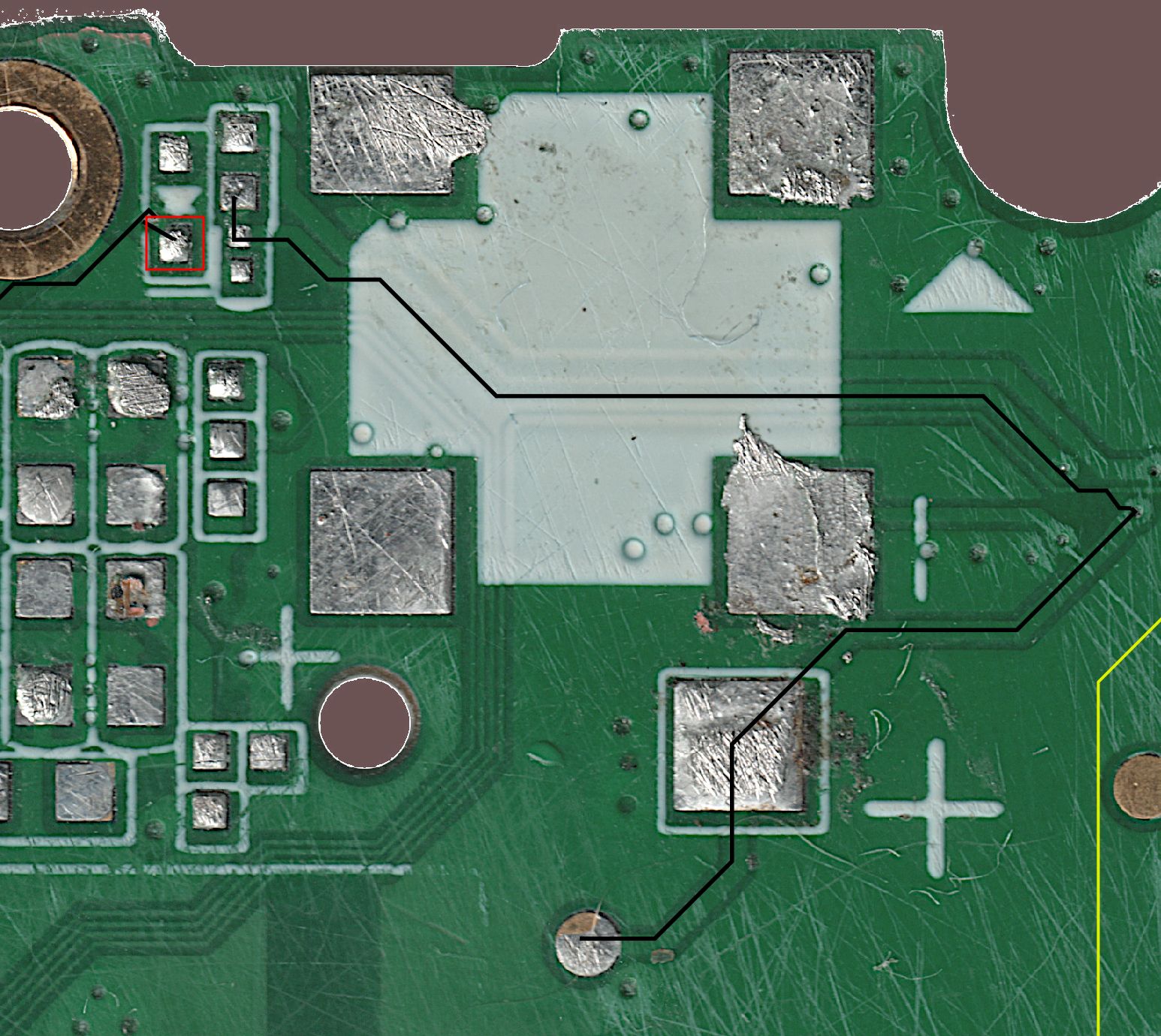
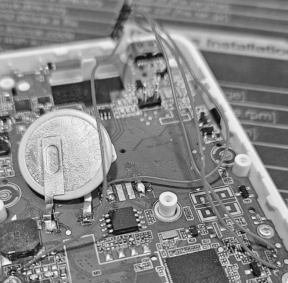
So looking at the D177 PCB, there is no specific test pad to actually act as a reset, but usually to avoid spending the coin cell battery energy when the power is supplied there is a series diode which I can use for soldering my reset wire. By tracing the pads I could find that the diode was in edge of the board.
So I just soldered a wire there, open my air105-uploader program and manually set it to GND and PROFIT
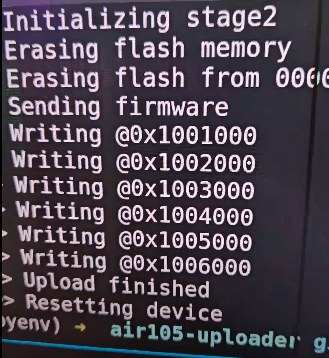 Now I could run code in the real machine!
Building code to it
I won’t get into much detail here (since this article is already getting bigger than I expected) but the TL;DR: LuatOS provides a way to build stuff, and has a “boiler plate” for initializing all the lua stuff. The CPU itself is a ARM Cortex so its easily buildable by GCC, just requiring a custom linker script to stitch everything in the right place.
Basically, I reused about everything I did for the AIR105, just changed the linker-script to be aware that MH1903 actually has 1MB of RAM instead 640KB. For making it easier to use, I created some platform.io libs that you can use directly.
If you want to try it, just install it through pip
pip install -U platformio
Then you can create a new project:
mkdir my-project && cd my-project
pio init
The following files/directories have been created in /tmp/m
include - Put project header files here
lib - Put project specific (private) libraries here
src - Put project source files here
platformio.ini - Project Configuration File
Project has been successfully initialized!
After that, you can just edit platformio.ini to map it to use the air105 platform:
[env:air105]
platform = https://github.com/racerxdl/platformio-air105
board = mh1903
framework = baremetal
;monitor_port = SERIAL_PORT
;monitor_speed = 115200
monitor_rts = 0 ; AIR105 board has inverted RTS
build_flags = -g -ggdb
You can change board parameter between mh1903 and air105 depending on what you’re targeting. The MH1903 is the 1MB variant, so code will crash on AIR105 due stack being positioned at the end of RAM space.
And for running:
pio run -t upload
This should build and upload (using the air105-uploader) directly. It will also download any toolchain and libs needed to do so. You can also add -t monitor to spawn a serial console and see the return from the machine.
The source code for the framework and platform on platform.io links are in the end of this article.
MAGIC STUFF
So, this article is getting huge and I feel lots of details will be badly written if I keep pushing content here. After all, this is like a 4 years+ research project. So I will eventually write two more articles about how I did map some magic stuff.
When I say magic stuff, next sections of this article will assume we know how the LCD is wired to the CPU, which I initially guessed it was in the same port as the flash memory we saw in the PCB. TL;DR it is, but not the Chip Select, neither the LCD backlight control, and these were not trivial to find since the LCD pinout is non-standard and I couldn’t find any datasheet of it.
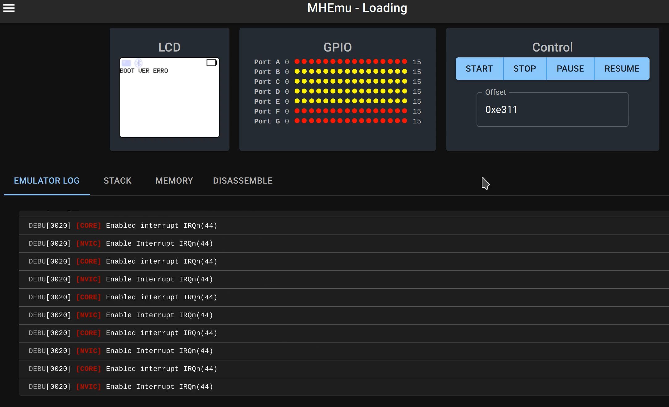
I did emulate the firmware to figure out some stuff (other stuff was just looking at decompiled sections) and the magic stuff I discovered is that the pins that control the LCD, are mapped into a GPIO that does not exists according to the datasheet 😃 (Spoiler, there are two undocumented GPIOs and few other stuff)
For now, let’s just pretend I wrote a nice article on how I did those. I promise I will write a new one with details on the reverse engineering and the details on how I made an emulator for it (that could even show the LCD images) 👀
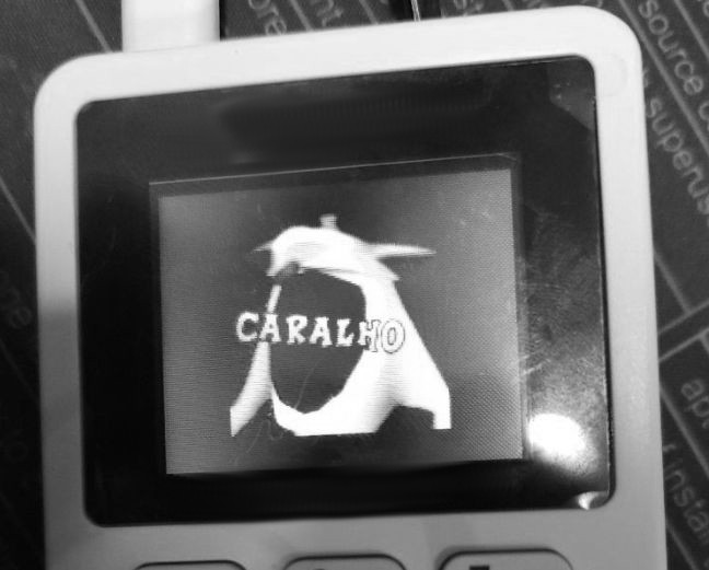
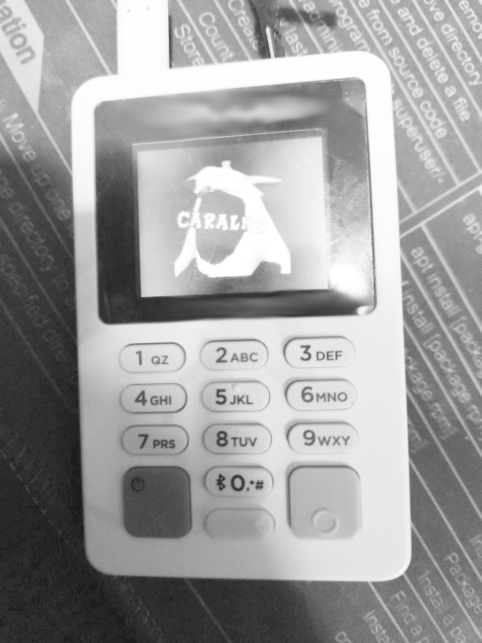
Making the “crasharalho”
The “crasharalho” is a sticker I use a lot in discord and telegram. “Caralho” is sort of the portuguese equivalent of “fuck” in the sense “OMG”. So the Crash Bandicoot screaming it on the machine, seem a perfect fit.
Making it was easy, just created a 160x128 image in GIMP and stamped the sticker there.
 Gimp is also nice that it can export directly to a C header, sort of compressed with a macro to actually get each R,G,B pixel values. So it was pretty easy to convert it.
/* GIMP header image file format (RGB): include/crasharalho.h */

static unsigned int width = 160;
static unsigned int height = 128;

/* Call this macro repeatedly. After each use, the pixel data can be extracted */

#define HEADER_PIXEL(data,pixel) {\
pixel[0] = (((data[0] - 33) << 2) | ((data[1] - 33) >> 4)); \
pixel[1] = ((((data[1] - 33) & 0xF) << 4) | ((data[2] - 33) >> 2)); \
pixel[2] = ((((data[2] - 33) & 0x3) << 6) | ((data[3] - 33))); \
data += 4; \
}

static const char *header_data =

")#!A)#!A)#!A)#!A)#!A)#!A)#!A)#!A)#!A)#!A)#!A)#!A)#!A)#!A)#!A)#!A"

")#!A)#!A)#!A)#!A)#!A)#!A)#!A)#!A)#!A)#!A)#!A)#!A)#!A)#!A)#!A)#!A"
(...)
The ST7735 LCD the machine uses has several pixel modes. I decided to use RGB565 since that would be exactly 16 bit wide (which gives two bytes over SPI) and easy to convert. I was lazy, so I used a local LLM to generate a macro to convert it, which worked pretty good (I didn’t remember how to convert the spaces, were not sure if was just cutting bits or actually a LUT)
#define RGB888_TO_RGB565(r, g, b) ( \
(((r) & 0xF8) << 8) | /* 5 bits of red, shifted to bits 15-11 */ \
(((g) & 0xFC) << 3) | /* 6 bits of green, shifted to bits 10-5 */ \
(((b) & 0xF8) >> 3) /* 5 bits of blue, shifted to bits 4-0 */ \
)
LLM generated a bit cut, and it worked nice. So I left as is. Then I could just send it in the code directly:
    {
        // 0x2C RAMWR
        SendCMD(LCD_SPI, 0x2C);                // RAMWR
        P15_ON;
        uint8_t rgb[3];
        // Fill the screen with white color // 16 bit mode
        for (int i = 0; i < 160 * 128; i++) {
            HEADER_PIXEL(header_data, rgb);
            uint16_t color = RGB888_TO_RGB565(rgb[0], rgb[1], rgb[2]);
            SendCMDParam(LCD_SPI,color >> 8); // Send high byte
            SendCMDParam(LCD_SPI, color & 0xFF); // Send low byte
        }
        P15_OFF;
    }
And tested it on my emulator:
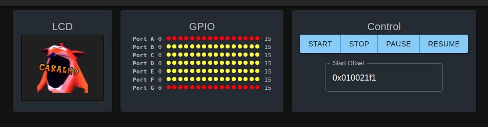
Result
Next steps
Running doom, of course :D - I planned of making this article only after doom, but I found out that the 1MB of ram, its sort of low for standard doom. I saw there is a RP2040 port of doom which works great, so I will probably port it to that core.
I still want to reverse engineer about everything I can from these SoCs, since they’re pretty powerful and has nice accelerators which can be used for some other secure stuff. I also managed to dump both MH1903S and MH1903 boot roms which has their own interesting aspects. I almost finished reversing engineering the MH1903S boot rom and I plan to make an article about it soon. It seens like that is several versions of boot roms around (they basically all do the same thing, but has different revisions and builds). So if you stumble across any MH190x device which you can either JTAG it or doesn’t have boot signature enabled. Let me know, lets make an archive of boot roms 😃
Notes
- There was a bit of research over both PAX and PagBank codes for finding out how it interacts with the hardware. No security flaw was explored and there is nothing they can do about the CPU swapping.
- There is nothing specific to PagBank in that case. Any D177 should work fine. The work here is not due a security flaw.
- Megahunt does a LOT of “Silicon OEM” (the AIR105 mentioned here is just one of them). Decaps should point out.
- Besides the boot rom, I don’t share binaries I dumped from machines. I hadn’t reverse engineer enough to know which info they store, and they might contain stuff that should be private. So please don’t ask, you can dump it yourself. Its pretty easy.
- Following articles will show how I reverse engineered the boot loaders, pax image format and found out how the LCD pins were mapped.
Links
- https://github.com/racerxdl/platformio-air105 - PIO Platform for AIR105/MH1903
- https://github.com/racerxdl/framework-megahunt - PIO Framework for Megahunt devices
- https://github.com/racerxdl/air105-uploader - Python script to upload using the boot rom
- https://archive.org/details/mh-1903-s-v-1.5 - Some useful MH1903 datasheets
- https://github.com/racerxdl/d177-crasharalho - Crasharalho Source Code
- https://github.com/racerxdl/megahunt-bootroms - Megahunt Bootroms
- https://github.com/racerxdl/mhdumper - Megahunt ROM Dumper Tool
Timeline
- 01/04/2025 - Resumed works on reverse-engineering and mapping
- 17/06/2025 - Got first code running (crasharalho)
- 22/06/2025 - Finished article, sent for peer review (tech-wise)
- 27/08/2025 - Send the article to Pag for review
- 28/08/2025 - Approved by Pag for publishing
- 31/08/2025 - More reviews, translation, etc…
- 05/09/2025 - Published